PIC18F6525/6621/8525/8621
When the Timer1 oscillator is enabled (T1OSCEN is
12.1 Timer1 Operation
set), the RC1/T1OSI and RC0/T1OSO/T13CKI pins
become inputs. That is, the TRISC<1:0> value is
ignored and the pins are read as ‘0’.
Timer1 can operate in one of these modes:
• As a timer
• As a synchronous counter
• As an asynchronous counter
Timer1 also has an internal “Reset input”. This Reset
can be generated by the ECCP1 or ECCP2 special
event trigger. This is discussed in detail in Section 12.4
“Resetting Timer1 Using an ECCP Special Trigger
Output”.
The operating mode is determined by the clock select
bit, TMR1CS (T1CON<1>).
When TMR1CS = 0, Timer1 increments every instruc-
tion cycle. When TMR1CS = 1, Timer1 increments on
every rising edge of the external clock input or the
Timer1 oscillator, if enabled.
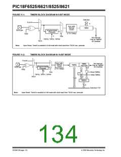
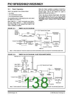
FIGURE 12-1:
TIMER1 BLOCK DIAGRAM
ECCP Special Event Trigger
TMR1IF
Overflow
Interrupt
Flag Bit
Synchronized
TMR1
CLR
0
Clock Input
TMR1L
TMR1H
1
TMR1ON
On/Off
T1SYNC
T1OSC
1
T1OSO/T13CKI
T1OSI
Synchronize
det
T1OSCEN
Enable
Oscillator
Prescaler
1, 2, 4, 8
FOSC/4
Internal
Clock
(1)
0
2
Sleep Input
T1CKPS1:T1CKPS0
TMR1CS
Note 1: When enable bit T1OSCEN is cleared, the inverter and feedback resistor are turned off. This eliminates power drain.
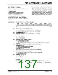
FIGURE 12-2:
TIMER1 BLOCK DIAGRAM: 16-BIT READ/WRITE MODE
Data Bus<7:0>
8
TMR1H
8
8
Write TMR1L
Read TMR1L
ECCP Special Event Trigger
TMR1IF
Overflow
Interrupt
Synchronized
Clock Input
TMR1
8
0
CLR
Timer 1
High Byte
TMR1L
Flag bit
1
TMR1ON
T1SYNC
On/Off
T1OSC
T1OSO/T13CKI
1
Synchronize
det
Prescaler
1, 2, 4, 8
T1OSCEN
FOSC/4
Internal
Clock
Enable
0
(1)
T1OSI
Oscillator
2
Sleep Input
TMR1CS
T1CKPS1:T1CKPS0
Note 1: When enable bit T1OSCEN is cleared, the inverter and feedback resistor are turned off. This eliminates power drain.
DS39612B-page 136
2005 Microchip Technology Inc.

 MICROCHIP [ MICROCHIP ]