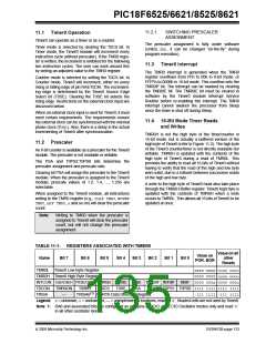
PIC18F6525/6621/8525/8621
12.2 Timer1 Oscillator
12.3 Timer1 Interrupt
A crystal oscillator circuit is built-in between pins T1OSI
(input) and T1OSO (amplifier output). It is enabled by
setting control bit T1OSCEN (T1CON<3>). The oscilla-
tor is a low-power oscillator rated up to 200 kHz. It will
continue to run during Sleep. It is primarily intended for
a 32 kHz crystal. The circuit for a typical LP oscillator is
shown in Figure 12-3. Table 12-1 shows the capacitor
selection for the Timer1 oscillator.
The TMR1 register pair (TMR1H:TMR1L) increments
from 0000h to FFFFh and rolls over to 0000h. The
TMR1 interrupt, if enabled, is generated on overflow
which is latched in interrupt flag bit, TMR1IF
(PIR1<0>). This interrupt can be enabled/disabled by
setting/clearing the TMR1 Interrupt Enable bit, TMR1IE
(PIE1<0>).
12.4 Resetting Timer1 Using an ECCP
Special Trigger Output
The user must provide a software time delay to ensure
proper start-up of the Timer1 oscillator.
If either the ECCP1 or ECCP2 module is configured in
Compare mode to generate a “special event trigger”
(CCP1M3:CCP1M0 = 1011), this signal will reset
Timer1. The trigger for ECCP2 will also start an A/D
conversion if the A/D module is enabled.
FIGURE 12-3:
EXTERNALCOMPONENTS
FOR THE TIMER1
LP OSCILLATOR
C1
33 pF
PIC18F6X2X/8X2X
Note:
The special event triggers from the
ECCP1 module will not set interrupt flag
bit TMR1IF (PIR1<0>).
T1OSI
XTAL
32.768 kHz
Timer1 must be configured for either Timer or Synchro-
nized Counter mode to take advantage of this feature.
If Timer1 is running in Asynchronous Counter mode,
this Reset operation may not work.
T1OSO
C2
33 pF
In the event that a write to Timer1 coincides with a
special event trigger from ECCP1, the write will take
precedence.
Note:
See the notes with Table 12-1 for additional
information about capacitor selection.
In this mode of operation, the CCPR1H:CCPR1L
register pair effectively becomes the period register for
Timer1.
TABLE 12-1: CAPACITOR SELECTION
FOR THE ALTERNATE
OSCILLATOR(2-4)
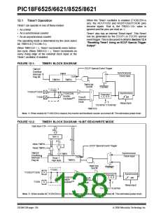
12.5 Timer1 16-Bit Read/Write Mode
Osc Type
Freq
C1
C2
Timer1 can be configured for 16-bit reads and writes
(see Figure 12-2). When the RD16 control bit
(T1CON<7>) is set, the address for TMR1H is mapped
to a buffer register for the high byte of Timer1. A read
from TMR1L will load the contents of the high byte of
Timer1 into the Timer1 High Byte Buffer register. This
provides the user with the ability to accurately read all
16 bits of Timer1 without having to determine whether
a read of the high byte, followed by a read of the low
byte, is valid due to a rollover between reads.
LP
32 kHz
15-22 pF(1) 15-22 pF(1)
Crystal Tested
32.768 kHz
Note 1: Microchip suggests 33 pF as a starting
point in validating the oscillator circuit.
2: Higher capacitance increases the stability
of the oscillator but also increases the
start-up time.
A write to the high byte of Timer1 must also take place
through the TMR1H Buffer register. Timer1 high byte is
updated with the contents of TMR1H when a write
occurs to TMR1L. This allows a user to write all 16 bits
to both the high and low bytes of Timer1 at once.
3: Since each resonator/crystal has its own
characteristics, the user should consult
the resonator/crystal manufacturer for
appropriate
values
of
external
The high byte of Timer1 is not directly readable or
writable in this mode. All reads and writes must take
place through the Timer1 High Byte Buffer register.
Writes to TMR1H do not clear the Timer1 prescaler.
The prescaler is only cleared on writes to TMR1L.
components.
4: Capacitor values are for design guidance
only.
2005 Microchip Technology Inc.
DS39612B-page 137

 MICROCHIP [ MICROCHIP ]