PIC18F6525/6621/8525/8621
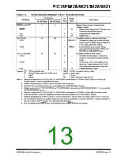
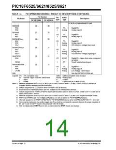
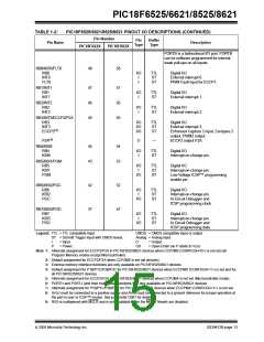
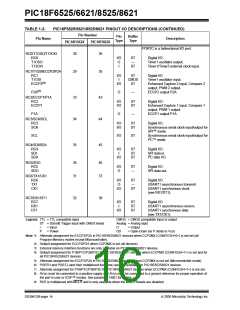
TABLE 1-2:
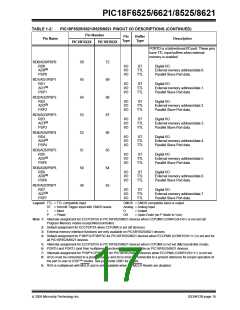
PIC18F6525/6621/8525/8621 PINOUT I/O DESCRIPTIONS
Pin Number
Pin
Type
Buffer
Type
Pin Name
Description
PIC18F6X2X
PIC18F8X2X
(9)
MCLR/VPP/RG5
MCLR
7
9
Master Clear (input) or programming
voltage (output).
I
ST
Master Clear (Reset) input. This pin is an
active-low Reset to the device.
Programming voltage input.
Digital input.
VPP
RG5
P
I
—
ST
OSC1/CLKI
OSC1
39
49
50
Oscillator crystal or external clock input.
Oscillator crystal input or external clock
source input. ST buffer when configured
in RC mode; otherwise CMOS.
I
I
CMOS/ST
CMOS
CLKI
External clock source input. Always
associated with pin function OSC1 (see
OSC1/CLKI, OSC2/CLKO pins).
OSC2/CLKO/RA6
OSC2
40
Oscillator crystal or clock output.
Oscillator crystal output. Connects to
crystal or resonator in Crystal oscillator
mode.
O
O
—
—
CLKO
RA6
In RC mode, OSC2 pin outputs CLKO
which has 1/4 the frequency of OSC1
and denotes the instruction cycle rate.
General purpose I/O pin.
I/O
TTL
Legend: TTL = TTL compatible input
ST = Schmitt Trigger input with CMOS levels
= Input
= Power
CMOS = CMOS compatible input or output
Analog = Analog input
I
P
O
= Output
OD
= Open-Drain (no P diode to VDD)
Note 1: Alternate assignment for ECCP2/P2A in PIC18F8525/8621 devices when CCP2MX (CONFIG3H<0>) is not set (all
Program Memory modes except Microcontroller).
2: Default assignment for ECCP2/P2A when CCP2MX is set (all devices).
3: External memory interface functions are only available on PIC18F8525/8621 devices.
4: Default assignment for P1B/P1C/P3B/P3C for PIC18F8525/8621 devices when ECCPMX (CONFIG3H<1>) is set and for
all PIC18F6525/6621 devices.
5: Alternate assignment for ECCP2/P2A in PIC18F8525/8621 devices when CCP2MX is not set (Microcontroller mode).
6: PORTH and PORTJ (and their multiplexed functions) are only available on PIC18F8525/8621 devices.
7: Alternate assignment for P1B/P1C/P3B/P3C for PIC18F8525/8621 devices when ECCPMX (CONFIG3H<1>) is not set.
8: AVDD must be connected to a positive supply and AVSS must be connected to a ground reference for proper operation of
the part in user or ICSP™ modes. See parameter D001 for details.
9: RG5 is multiplexed with MCLR and is only available when the MCLR Resets are disabled.
2005 Microchip Technology Inc.
DS39612B-page 11

 MICROCHIP [ MICROCHIP ]