PIC18F6525/6621/8525/8621
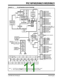
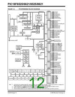
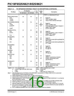
FIGURE 1-2:
PIC18F8525/8621 BLOCK DIAGRAM
PORTA
PORTB
Data Bus<8>
RA0/AN0
RA1/AN1
RA2/AN2/VREF-
RA3/AN3/VREF+
RA4/T0CKI
RA5/AN4/LVDIN
OSC2/CLKO/RA6
Table Pointer<21>
inc/dec logic
Data Latch
21
8
8
Data RAM
(3.8 Kbytes)
21
Address Latch
12
RB0/INT0/FLT0
RB1/INT1
20
PCLATU PCLATH
RB2/INT2
Address<12>
RB3/INT3/ECCP2(1)/P2A(1)
RB4/KBI0
PCU PCH PCL
Program Counter
12
FSR0
4
4
RB5/KBI1/PGM
RB6/KBI2/PGC
RB7/KBI3/PGD
BSR
Bank0, F
Address Latch
FSR1
FSR2
Program Memory
(48/64 Kbytes)
31 Level Stack
12
PORTC
RC0/T1OSO/T13CKI
RC1/T1OSI/ECCP2(1)/P2A(1)
RC2/ECCP1/P1A
RC3/SCK/SCL
RC4/SDI/SDA
RC5/SDO
RC6/TX1/CK1
RC7/RX1/DT1
Data Latch
inc/dec
logic
Decode
Table Latch
8
16
ROM Latch
IR
PORTD
PORTE
(4)
RD7/AD7/PSP7:
RD0/AD0/PSP0(4)
AD15:AD0, A19:16
8
RE0/AD8/RD/P2D(4)
RE1/AD9/WR/P2C(4)
RE2/AD10/CS/P2B(4)
RE3/AD11/P3C(2,4)
RE4/AD12/P3B(2,4)
RE5/AD13/P1C(2,4)
RE6/AD14/P1B(2,4)
RE7/AD15/ECCP2(1)/P2A(1,4)
PRODH PRODL
8 x 8 Multiply
Instruction
Decode and
Control
8
3
W
8
BITOP
8
8
Power-up
OSC2/CLKO
OSC1/CLKI
Timer
PORTF
Timing
Oscillator
Start-up Timer
RF0/AN5
8
Generation
RF1/AN6/C2OUT
RF2/AN7/C1OUT
RF3/AN8
ALU<8>
Power-on
Reset
RF4/AN9
RF5/AN10/CVREF
RF6/AN11
8
Watchdog
Timer
Precision
Band Gap
Reference
Brown-out
Reset
RF7/SS
PORTG
Test Mode
Select
RG0/ECCP3/P3A
RG1/TX2/CK2
RG2/RX2/DT2
RG3/CCP4/P3D
RG4/CCP5/P1D
MCLR/VPP/RG5(3)
MCLR(3)
Timer2
VDD, VSS
Timer1
PORTH
PORTJ
RH0/A16:RH3/A19(4)
RH4/AN12/P3C(2)
RH5/AN13/P3B(2)
RH6/AN14/P1C(2)
RH7/AN15/P1B(2)
Data
EEPROM
BOR
LVD
10-bit
Timer4
Timer0
Timer3
ADC
RJ0/ALE
RJ1/OE
RJ2/WRL
RJ3/WRH
RJ4/BA0
RJ5/CE
RJ6/LB
MSSP
Comparator ECCP1 ECCP2 ECCP3 CCP4 CCP5
EUSART1 EUSART2
RJ7/UB
Note 1: ECCP2/P2A are multiplexed with RC1 when CCP2MX is set; with RE7 when CCP2MX is cleared and the device is configured in
Microcontroller mode; or with RB3 when CCP2MX is cleared in all other program memory modes.
2: P1B/P1C/P3B/P3C are multiplexed with RE6:RE3 when ECCPMX is set and with RH7:RH4 when ECCPMX is not set.
3: RG5 is multiplexed with MCLR and is only available when the MCLR Resets are disabled.
4: External memory interface pins are multiplexed with PORTD (AD7:AD0), PORTE (AD15:AD8) and PORTH (A19:A16).
DS39612B-page 10
2005 Microchip Technology Inc.

 MICROCHIP [ MICROCHIP ]