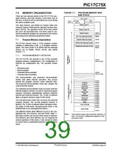
PIC17C75X
6.4
Interrupt Operation
6.5
RA0/INT Interrupt
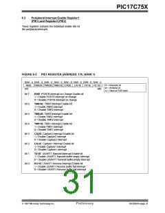
Global Interrupt Disable bit, GLINTD (CPUSTA<4>),
enables all unmasked interrupts (if clear) or disables all
interrupts (if set). Individual interrupts can be disabled
through their corresponding enable bits in the INTSTA
register. Peripheral interrupts need either the global
peripheral enable PEIE bit disabled, or the specific
peripheral enable bit disabled. Disabling the peripher-
als via the global peripheral enable bit, disables all
peripheral interrupts. GLINTD is set on reset (interrupts
disabled).
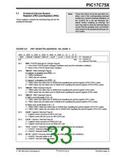
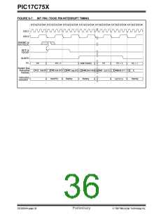
The external interrupt on the RA0/INT pin is edge trig-
gered. Either the rising edge, if INTEDG bit
(T0STA<7>) is set, or the falling edge, if INTEDG bit is
clear. When a valid edge appears on the RA0/INT pin,
the INTF bit (INTSTA<4>) is set. This interrupt can be
disabled by clearing the INTE control bit (INTSTA<0>).
The INT interrupt can wake the processor from SLEEP.
See Section 17.4 for details on SLEEP operation.
6.6
T0CKI Interrupt
The RETFIEinstruction allows returning from interrupt
and re-enables interrupts at the same time.
The external interrupt on the RA1/T0CKI pin is edge
triggered. Either the rising edge, if the T0SE bit
(T0STA<6>) is set, or the falling edge, if the T0SE bit is
clear. When a valid edge appears on the RA1/T0CKI
pin, the T0CKIF bit (INTSTA<6>) is set. This interrupt
can be disabled by clearing the T0CKIE control bit
(INTSTA<2>). The T0CKI interrupt can wake up the
processor from SLEEP. See Section 17.4 for details on
SLEEP operation.
When an interrupt is responded to, the GLINTD bit is
automatically set to disable any further interrupt, the
return address is pushed onto the stack and the PC is
loaded with the interrupt vector.There are four interrupt
vectors which help reduce interrupt latency.
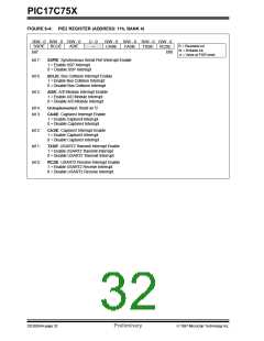
The peripheral interrupt vector has multiple interrupt
sources. Once in the peripheral interrupt service rou-
tine, the source(s) of the interrupt can be determined by
polling the interrupt flag bits. The peripheral interrupt
flag bit(s) must be cleared in software before
re-enabling interrupts to avoid continuous interrupts.
6.7
Peripheral Interrupt
The peripheral interrupt flag indicates that at least one
of the peripheral interrupts occurred (PEIF is set). The
PEIF bit is a read only bit, and is a bit wise OR of all the
flag bits in the PIR registers AND’ed with the corre-
sponding enable bits in the PIE registers. Some of the
peripheral interrupts can wake the processor from
SLEEP. See Section 17.4 for details on SLEEP opera-
tion.
The PIC17C75X devices have four interrupt vectors.
These vectors and their hardware priority are shown in
Table 6-1. If two enabled interrupts occur “at the same
time”, the interrupt of the highest priority will be ser-
viced first. This means that the vector address of that
interrupt will be loaded into the program counter (PC).
6.8
Context Saving During Interrupts
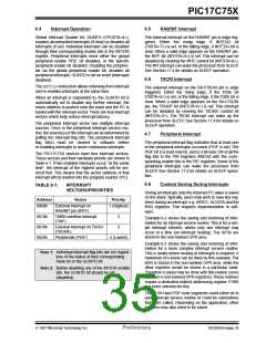
TABLE 6-1:
INTERRUPT
VECTORS/PRIORITIES
During an interrupt, only the returned PC value is saved
on the stack.Typically, users may wish to save key reg-
isters during an interrupt; e.g. WREG, ALUSTA and the
BSR registers. This requires implementation in soft-
ware.
Address
Vector
Priority
0008h
0010h
0018h
0020h
External Interrupt on
RA0/INT pin (INTF)
1 (Highest)
TMR0 overflow interrupt
(T0IF)
2
3
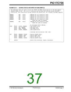
Example 6-2 shows the saving and restoring of infor-
mation for an interrupt service routine.This is for a sim-
ple interrupt scheme, where only one interrupt may
occur at a time (no interrupt nesting). The SFRs are
stored in the non-banked GPR area.
External Interrupt on T0CKI
(T0CKIF)
Peripherals (PEIF)
4 (Lowest)
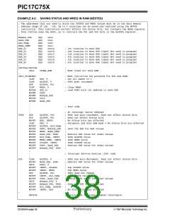
Example 6-2 shows the saving and restoring of infor-
mation for a more complex interrupt service routine.
This is useful where nesting of interrupts is required. A
maximum of 6 levels can be done by this example. The
BSR is stored in the non-banked GPR area, while the
other registers would be stored in a particular bank.
Therefore 6 saves may be done with this routine (since
there are 6 non-banked GPR registers).These routines
require a dedicated indirect addressing register, FSR0
has been selected for this.
Note 1: Individual interrupt flag bits are set regard-
less of the status of their corresponding
mask bit or the GLINTD bit.
Note 2: Before disabling any of the INTSTA enable
bits, the GLINTD bit should be set
(disabled).
The PUSH and POP code segments could either be in
each interrupt service routine or could be subroutines
that were called. Depending on the application, other
registers may also need to be saved.
1997 Microchip Technology Inc.
Preliminary
DS30264A-page 35

 MICROCHIP [ MICROCHIP ]