PIC17C4X
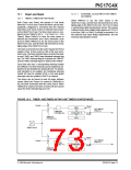
Timer3 is a 16-bit timer/counter consisting of the
TMR3H and TMR3L registers.This timer has four other
associated registers.Two registers are used as a 16-bit
12.0 TIMER1, TIMER2,TIMER3,
PWMS AND CAPTURES
The PIC17C4X has a wealth of timers and time-based
functions to ease the implementation of control applica-
tions.These time-base functions include two PWM out-
puts and two Capture inputs.
period register or
a
16-bit Capture1 register
(PR3H/CA1H:PR3L/CA1L).The other two registers are
strictly the Capture2 registers (CA2H:CA2L). Timer3 is
the time-base for the two 16-bit captures.
Timer1 and Timer2 are two 8-bit incrementing timers,
each with a period register (PR1 and PR2 respectively)
and separate overflow interrupt flags. Timer1 and
Timer2 can operate either as timers (increment on
internal Fosc/4 clock) or as counters (increment on fall-
ing edge of external clock on pin RB4/TCLK12). They
are also software configurable to operate as a single
16-bit timer. These timers are also used as the
time-base for the PWM (pulse width modulation) mod-
ule.
TMR3 can be software configured to increment from
the internal system clock or from an external signal on
the RB5/TCLK3 pin.
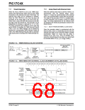
Figure 12-1 and Figure 12-2 are the control registers
for the operation of Timer1, Timer2, and Timer3, as well
as PWM1, PWM2, Capture1, and Capture2.
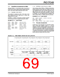
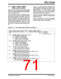
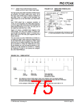
FIGURE 12-1: TCON1 REGISTER (ADDRESS: 16h, BANK 3)
R/W - 0 R/W - 0 R/W - 0 R/W - 0 R/W - 0 R/W - 0 R/W - 0 R/W - 0
R = Readable bit
W = Writable bit
-n = Value at POR reset
CA2ED1 CA2ED0 CA1ED1 CA1ED0
T16
TMR3CS TMR2CS TMR1CS
bit7
bit0
bit 7-6: CA2ED1:CA2ED0: Capture2 Mode Select bits
00 = Capture on every falling edge
01 = Capture on every rising edge
10 = Capture on every 4th rising edge
11 = Capture on every 16th rising edge
bit 5-4: CA1ED1:CA1ED0: Capture1 Mode Select bits
00 = Capture on every falling edge
01 = Capture on every rising edge
10 = Capture on every 4th rising edge
11 = Capture on every 16th rising edge
bit 3:
bit 2:
bit 1:
bit 0:
T16: Timer1:Timer2 Mode Select bit
1 = Timer1 and Timer2 form a 16-bit timer
0 = Timer1 and Timer2 are two 8-bit timers
TMR3CS: Timer3 Clock Source Select bit
1 = TMR3 increments off the falling edge of the RB5/TCLK3 pin
0 = TMR3 increments off the internal clock
TMR2CS: Timer2 Clock Source Select bit
1 = TMR2 increments off the falling edge of the RB4/TCLK12 pin
0 = TMR2 increments off the internal clock
TMR1CS: Timer1 Clock Source Select bit
1 = TMR1 increments off the falling edge of the RB4/TCLK12 pin
0 = TMR1 increments off the internal clock
1996 Microchip Technology Inc.
DS30412C-page 71
This document was created with FrameMaker 4 0 4

 MICROCHIP [ MICROCHIP ]