PIC17C4X
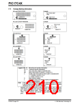
APPENDIX A:MODIFICATIONS
APPENDIX B:COMPATIBILITY
The following is the list of modifications over the
PIC16CXX microcontroller family:
To convert code written for PIC16CXX to PIC17CXX,
the user should take the following steps:
1. Instruction word length is increased to 16-bit.
This allows larger page sizes both in program
memory (8 Kwords verses 2 Kwords) and regis-
ter file (256 bytes versus 128 bytes).
1. Remove any TRIS and OPTION instructions,
and implement the equivalent code.
2. Separate the interrupt service routine into its
four vectors.
2. Four modes of operation: microcontroller, pro-
tected microcontroller, extended microcontroller,
and microprocessor.
3. Replace:
MOVF
with:
REG1, W
3. 22 new instructions.
MOVFP
REG1, WREG
The MOVF, TRISand OPTIONinstructions have
been removed.
4. Replace:
MOVF
REG1, W
REG2
4. 4 new instructions for transferring data between
data memory and program memory.This can be
used to “self program” the EPROM program
memory.
MOVWF
with:
MOVPF
or
REG1, REG2 ; Addr(REG1)<20h
MOVFP
REG1, REG2 ; Addr(REG2)<20h
5. Single cycle data memory to data memory trans-
fers possible (MOVPF and MOVFP instructions).
These instructions do not affect the Working reg-
ister (WREG).
Note: If REG1 and REG2 are both at addresses
greater then 20h, two instructions are
required.
6. W register (WREG) is now directly addressable.
MOVFP
MOVPF
REG1, WREG ;
WREG, REG2 ;
7. A PC high latch register (PCLATH) is extended
to 8-bits. The PCLATCH register is now both
readable and writable.
5. Ensure that all bit names and register names are
updated to new data memory map location.
8. Data memory paging is redefined slightly.
6. Verify data memory banking.
9. DDR registers replaces function of TRIS regis-
ters.
7. Verify mode of operation for indirect addressing.
8. Verify peripheral routines for compatibility.
9. Weak pull-ups are enabled on reset.
10. Multiple Interrupt vectors added. This can
decrease the latency for servicing the interrupt.
To convert code from the PIC17C42 to all the other
PIC17C4X devices, the user should take the following
steps.
11. Stack size is increased to 16 deep.
12. BSR register for data memory paging.
13. Wake up from SLEEP operates slightly differ-
ently.
1. If the hardware multiply is to be used, ensure
that any variables at address 18h and 19h are
moved to another address.
14. The Oscillator Start-Up Timer (OST) and
Power-Up Timer (PWRT) operate in parallel and
not in series.
2. Ensure that the upper nibble of the BSR was not
written with a non-zero value. This may cause
unexpected operation since the RAM bank is no
longer 0.
15. PORTB interrupt on change feature works on all
eight port pins.
16. TMR0 is 16-bit plus 8-bit prescaler.
3. The disabling of global interrupts has been
enhanced so there is no additional testing of the
GLINTD bit after a BSF CPUSTA, GLINTD
instruction.
17. Second indirect addressing register added
(FSR1 and FSR2). Configuration bits can select
the FSR registers to auto-increment, auto-dec-
rement, remain unchanged after an indirect
address.
18. Hardware multiplier added (8 x 8 → 16-bit)
(PIC17C43 and PIC17C44 only).
19. Peripheral modules operate slightly differently.
20. Oscillator modes slightly redefined.
21. Control/Status bits and registers have been
placed in different registers and the control bit
for globally enabling interrupts has inverse
polarity.
22. Addition of a test mode pin.
23. In-circuit serial programming is not imple-
mented.
1996 Microchip Technology Inc.
DS30412C-page 211
This document was created with FrameMaker 4 0 4

 MICROCHIP [ MICROCHIP ]