PIC17C4X
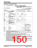
Applicable Devices 42 R42 42A 43 R43 44
17.2
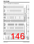
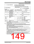
DC CHARACTERISTICS:
PIC17C42-16 (Commercial, Industrial)
PIC17C42-25 (Commercial, Industrial)
Standard Operating Conditions (unless otherwise stated)
Operating temperature
-40˚C ≤ TA ≤ +85˚C for industrial and
0˚C ≤ TA ≤ +70˚C for commercial
Operating voltage VDD range as described in Section 17.1
DC CHARACTERISTICS
Parameter
No.
Sym
Characteristic
Input Low Voltage
I/O ports
with TTL buffer
Min
Typ†
Max Units
Conditions
VIL
D030
D031
VSS
VSS
–
–
0.8
V
V
with Schmitt Trigger buffer
0.2VDD
D032
MCLR, OSC1 (in EC and RC
mode)
OSC1 (in XT, and LF mode)
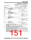
Input High Voltage
I/O ports
with TTL buffer
with Schmitt Trigger buffer
MCLR
Vss
–
0.2VDD
V
Note1
Note1
D033
–
0.5VDD
–
V
VIH
–
–
–
D040
D041
D042
D043
D050
2.0
0.8VDD
0.8VDD
–
VDD
VDD
VDD
–
V
V
V
V
V
–
0.5VDD
–
OSC1 (XT, and LF mode)
VHYS Hysteresis of
Schmitt Trigger inputs
0.15VDD*
–
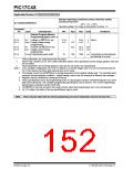
Input Leakage Current
(Notes 2, 3)
D060
IIL
I/O ports (except RA2, RA3)
–
–
±1
µA Vss ≤ VPIN ≤ VDD,
I/O Pin at hi-impedance
PORTB weak pull-ups dis-
abled
D061
D062
D063
D064
MCLR
–
–
±2
±2
±1
10
µA VPIN = Vss or VPIN = VDD
µA Vss ≤ VRA2, VRA3 ≤ 12V
µA Vss ≤ VPIN ≤ VDD
RA2, RA3
OSC1, TEST
MCLR
–
–
–
–
µA VMCLR = VPP = 12V
(when not programming)
D070
IPURB PORTB weak pull-up current
60
200
400
µA VPIN = VSS, RBPU = 0
*
These parameters are characterized but not tested.
†
Data in “Typ” column is at 5V, 25°C unless otherwise stated. These parameters are for design guidance only
and are not tested.
‡
††
These parameters are for design guidance only and are not tested, nor characterized.
Design guidance to attain the AC timing specifications. These loads are not tested.
Note 1: In RC oscillator configuration, the OSC1 pin is a Schmitt Trigger input. It is not recommended that the
PIC17CXX devices be driven with external clock in RC mode.
2: The leakage current on the MCLR pin is strongly dependent on the applied voltage level. The specified levels
represent normal operating conditions. Higher leakage current may be measured at different input voltages.
3: Negative current is defined as coming out of the pin.
4: These specifications are for the programming of the on-chip program memory EPROM through the use of the
table write instructions. The complete programming specifications can be found in: PIC17CXX Programming
Specifications (Literature number DS30139).
5: The MCLR/Vpp pin may be kept in this range at times other than programming, but this is not recommended.
6: For TTL buffers, the better of the two specifications may be used.
DS30412C-page 150
1996 Microchip Technology Inc.

 MICROCHIP [ MICROCHIP ]