PIC17C75X
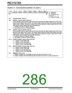
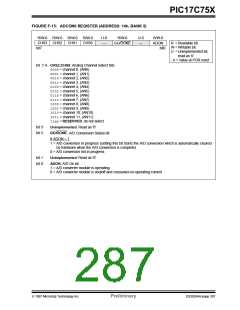
FIGURE F-15: ADCON0 REGISTER (ADDRESS: 14h, BANK 5)
R/W-0 R/W-0 R/W-0
CHS3 CHS2 CHS1
bit7
R/W-0
CHS0
U-0
—
R/W-0
U-0
—
R/W-0
ADON
GO/DONE
R =Readable bit
W = Writable bit
U =Unimplemented bit,
read as ‘0’
bit0
- n = Value at POR reset
bit 7-4: CHS2:CHS0: Analog Channel Select bits
0000= channel 0, (AN0)
0001= channel 1, (AN1)
0010= channel 2, (AN2)
0011= channel 3, (AN3)
0100= channel 4, (AN4)
0101= channel 5, (AN5)
0110= channel 6, (AN6)
0111= channel 7, (AN7)
1000= channel 8, (AN8)
1001= channel 9, (AN9)
1010= channel 10, (AN10)
1011= channel 11, (AN11)
11xx= RESERVED, do not select
bit 3:
bit 2:
Unimplemented: Read as '0'
GO/DONE: A/D Conversion Status bit
If ADON = 1
1 = A/D conversion in progress (setting this bit starts the A/D conversion which is automatically cleared
by hardware when the A/D conversion is complete)
0 = A/D conversion not in progress
bit 1:
bit 0:
Unimplemented: Read as '0'
ADON: A/D On bit
1 = A/D converter module is operating
0 = A/D converter module is shutoff and consumes no operating current
1997 Microchip Technology Inc.
Preliminary
DS30264A-page 287

 MICROCHIP [ MICROCHIP ]