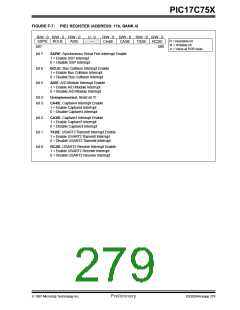
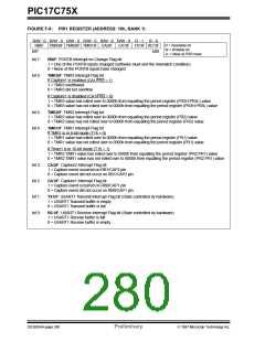
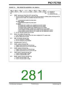
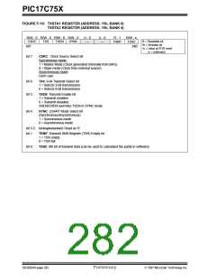
PIC17C75X
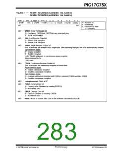
FIGURE F-11: RCSTA1 REGISTER (ADDRESS: 13h, BANK 0)
RCSTA2 REGISTER (ADDRESS: 13h, BANK 4)
R/W - 0 R/W - 0 R/W - 0 R/W - 0
SPEN RX9 SREN CREN
bit7
U - 0
—
R - 0
FERR
R - 0
OERR
R - x
RX9D
R = Readable bit
W = Writable bit
-n = Value at POR reset
(x = unknown)
bit 0
bit 7:
bit 6:
bit 5:
SPEN: Serial Port Enable bit
1 = Configures TX/CK and RX/DT pins as serial port pins
0 = Serial port disabled
RX9: 9-bit Receive Select bit
1 = Selects 9-bit reception
0 = Selects 8-bit reception
SREN: Single Receive Enable bit
This bit enables the reception of a single byte. After receiving the byte, this bit is automatically cleared.
Synchronous mode:
1 = Enable reception
0 = Disable reception
Note: This bit is ignored in synchronous slave reception.
Asynchronous mode:
Don’t care
bit 4:
CREN: Continuous Receive Enable bit
This bit enables the continuous reception of serial data.
Asynchronous mode:
1 = Enable continuous reception
0 = Disables continuous reception
Synchronous mode:
1 = Enables continuous reception until CREN is cleared (CREN overrides SREN)
0 = Disables continuous reception
bit 3:
bit 2:
Unimplemented: Read as '0'
FERR: Framing Error bit
1 = Framing error (Updated by reading RCREG)
0 = No framing error
bit 1:
bit 0:
OERR: Overrun Error bit
1 = Overrun (Cleared by clearing CREN)
0 = No overrun error
RX9D: 9th bit of receive data (can be the software calculated parity bit)
1997 Microchip Technology Inc.
Preliminary
DS30264A-page 283

 MICROCHIP [ MICROCHIP ]