PIC17C75X
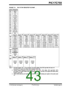
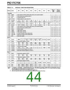
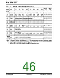
TABLE 7-3:
SPECIAL FUNCTION REGISTERS
Value on
POR,
BOR
Value on
all other
resets (3)
Address Name
Bit 7
Bit 6
Bit 5
Bit 4
Bit 3
Bit 2
Bit 1
Bit 0
Unbanked
00h
01h
02h
INDF0
FSR0
Uses contents of FSR0 to address data memory (not a physical register)
Indirect data memory address pointer 0
Low order 8-bits of PC
---- ---- ---- ----
xxxx xxxx uuuu uuuu
0000 0000 0000 0000
0000 0000 uuuu uuuu
PCL
03h(1)
04h
PCLATH
ALUSTA
T0STA
Holding register for upper 8-bits of PC
FS3
FS2
FS1
FS0
OV
Z
DC
C
1111 xxxx 1111 uuuu
0000 000- 0000 000-
05h
INTEDG
T0SE
T0CS
T0PS3
T0PS2
T0PS1
T0PS0
—
06h(2)
07h
—
—
STKAV
T0IF
GLINTD
INTF
TO
PD
POR
T0IE
BOR
INTE
--11 1100 --11 qquu
CPUSTA
INTSTA
INDF1
PEIF
T0CKIF
PEIE
T0CKIE
0000 0000 0000 0000
---- ---- ---- ----
xxxx xxxx uuuu uuuu
xxxx xxxx uuuu uuuu
xxxx xxxx uuuu uuuu
xxxx xxxx uuuu uuuu
0000 0000 0000 0000
0000 0000 0000 0000
0000 0000 0000 0000
08h
Uses contents of FSR1 to address data memory (not a physical register)
Indirect data memory address pointer 1
Working register
09h
FSR1
0Ah
0Bh
0Ch
0Dh
0Eh
0Fh
WREG
TMR0L
TMR0H
TBLPTRL
TBLPTRH
BSR
TMR0 register; low byte
TMR0 register; high byte
Low byte of program memory table pointer
High byte of program memory table pointer
Bank select register
Bank 0
10h
RA5/TX1/ RA4/RX1/ RA3/SDI/ RA2/SS/
PORTA
DDRB
RBPU
—
RA1/T0CKI RA0/INT 0-xx xxxx 0-uu uuuu
CK1
Data direction register for PORTB
DT1
SDA
SCL
11h
1111 1111 1111 1111
RB7/
SDO
RB6/
SCK
RB5/
TCLK3
RB4/
TCLK12
RB3/
PWM2
RB2/
PWM1
RB1/
CAP2
RB0/
CAP1
12h
PORTB
xxxx xxxx uuuu uuuu
13h
14h
15h
16h
17h
RCSTA1
RCREG1
TXSTA1
TXREG1
SPBRG1
SPEN
RX9
SREN
CREN
—
—
FERR
—
OERR
TRMT
RX9D
TX9D
0000 -00x 0000 -00u
xxxx xxxx uuuu uuuu
0000 --1x 0000 --1u
xxxx xxxx uuuu uuuu
xxxx xxxx uuuu uuuu
Serial port receive register
CSRC TX9 TXEN
SYNC
Serial Port Transmit Register (for USART1)
Baud Rate Generator Register (for USART1)
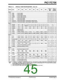
Bank 1
10h
DDRC
PORTC
DDRD
PORTD
DDRE
Data direction register for PORTC
1111 1111 1111 1111
xxxx xxxx uuuu uuuu
1111 1111 1111 1111
xxxx xxxx uuuu uuuu
---- 1111 ---- 1111
RC7/
AD7
RC6/
AD6
RC5/
AD5
RC4/
AD4
RC3/
AD3
RC2/
AD2
RC1/
AD1
RC0/
AD0
11h
12h
13h
14h
15h
Data direction register for PORTD
RD7/
AD15
RD6/
AD14
RD5/
AD13
RD4/
AD12
RD3/
AD11
RD2/
AD10
RD1/
AD9
RD0/
AD8
Data direction register for PORTE
RE3/
CAP4
PORTE
—
—
—
—
RE2/WR
RE1/OE
RE0/ALE ---- xxxx ---- uuuu
16h
17h
PIR1
PIE1
RBIF
RBIE
TMR3IF
TMR2IF
TMR1IF
TMR1IE
CA2IF
CA2IE
CA1IF
CA1IE
TX1IF
TX1IE
RC1IF
RC1IE
x000 0010 u000 0010
0000 0000 0000 0000
TMR3IE TMR2IE
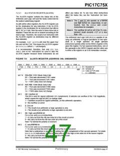
Legend:
Note 1:
x = unknown, u = unchanged, - = unimplemented read as '0', q - value depends on condition. Shaded cells are unimplemented, read as '0'.
The upper byte of the program counter is not directly accessible. PCLATH is a holding register for PC<15:8> whose contents are updated
from or transferred to the upper byte of the program counter.
2: The TO and PD status bits in CPUSTA are not affected by a MCLR reset.
3: Other (non power-up) resets include: external reset through MCLR and Watchdog Timer Reset.
DS30264A-page 44
Preliminary
1997 Microchip Technology Inc.

 MICROCHIP [ MICROCHIP ]