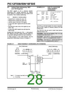
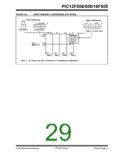
PIC12F508/509/16F505
TABLE 5-1:
SUMMARY OF PORT REGISTERS
Value on
Power-On
Reset
Value on
All Other
Resets
Address
Name
Bit 7
Bit 6
Bit 5
Bit 4
Bit 3
Bit 2
Bit 1 Bit 0
(1)
N/A
TRISGPIO
—
—
—
—
I/O Control Register
I/O Control Register
I/O Control Register
--11 1111
--11 1111
--11 1111
1111 1111
1111 1111
--11 1111
--11 1111
--11 1111
1111 1111
1111 1111
(2)
N/A
TRISB
(2)
N/A
TRISC
—
—
(1)
N/A
OPTION
GPWU
RBWU
GPWUF
RBWUF
—
GPPU
RBPU
—
TOCS
TOCS
PAO
PAO
GP5
TOSE
TOSE
TO
PSA
PSA
PD
PS2
PS2
Z
PS1
PS1
DC
PS0
PS0
C
(2)
N/A
OPTION
(1)
(3)
03h
STATUS
0-01 1xxx q00q quuu
0-01 1xxx q00q quuu
(2)
(3)
03h
STATUS
—
TO
PD
Z
DC
C
(1)
06h
GPIO
—
GP4
RB4
RC4
GP3
RB3
RC3
GP2
RB2
RC2
GP1
RB1
RC1
GP0
RB0
RC0
--xxxxxx
--xxxxxx
--xx xxxx
--uu uuuu
(2)
06h
PORTB
—
—
RB5
--uu uuuu
--uu uuuu
(2)
07h
PORTC
—
—
RC5
Legend:
Shaded cells are not used by Port registers, read as ‘0’. – = unimplemented, read as ‘0’, x= unknown, u= unchanged,
q= depends on condition.
Note 1: PIC12F508/509 only.
2: PIC16F505 only.
3: If Reset was due to wake-up on pin change, then bit 7 = 1. All other Resets will cause bit 7 = 0.
DS41236C-page 30
Preliminary
© 2007 Microchip Technology Inc.

 MICROCHIP [ MICROCHIP ]