PIC16F870/871
TABLE 1-2:
PIC16F871 PINOUT DESCRIPTION
DIP
Pin#
PLCC
Pin#
QFP
Pin#
I/O/P
Type
Buffer
Type
Pin Name
Description
(4)
OSC1/CLKIN
13
14
14
15
30
31
I
Oscillator crystal input/external clock source input.
ST/CMOS
OSC2/CLKOUT
O
—
Oscillator crystal output. Connects to crystal or resonator in
crystal oscillator mode. In RC mode, OSC2 pin outputs CLK-
OUT which has 1/4 the frequency of OSC1, and denotes the
instruction cycle rate.
MCLR/VPP/THV
1
2
18
I/P
ST
Master clear (reset) input or programming voltage input or high
voltage test mode control. This pin is an active low reset to the
device.
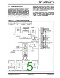
PORTA is a bi-directional I/O port.
RA0 can also be analog input0
RA1 can also be analog input1
RA0/AN0
2
3
4
3
4
5
19
20
21
I/O
I/O
I/O
TTL
TTL
TTL
RA1/AN1
RA2/AN2/VREF-
RA2 can also be analog input2 or negative analog
reference voltage
RA3/AN3/VREF+
RA4/T0CKI
RA5/AN4
5
6
7
6
7
8
22
23
24
I/O
I/O
I/O
TTL
ST
RA3 can also be analog input3 or positive analog
reference voltage
RA4 can also be the clock input to the Timer0 timer/
counter. Output is open drain type.
TTL
RA5 can also be analog input4
PORTB is a bi-directional I/O port. PORTB can be software
programmed for internal weak pull-up on all inputs.
(1)
RB0/INT
33
36
8
I/O
RB0 can also be the external interrupt pin.
TTL/ST
TTL
RB1
34
35
36
37
38
39
9
I/O
I/O
I/O
RB2
10
11
TTL
(1)
RB3/PGM
RB3 can also be the low voltage programming input
TTL/ST
TTL
RB4
37
38
39
41
42
43
14
15
16
I/O
I/O
I/O
Interrupt on change pin.
Interrupt on change pin.
RB5
TTL
(2)
(2)
RB6/PGC
Interrupt on change pin or In-Circuit Debugger pin. Serial
programming clock.
TTL/ST
RB7/PGD
40
15
44
16
17
32
I/O
I/O
Interrupt on change pin or In-Circuit Debugger pin. Serial
programming data.
TTL/ST
PORTC is a bi-directional I/O port.
RC0/T1OSO/T1CKI
ST
RC0 can also be the Timer1 oscillator output or a Timer1
clock input.
RC1/T1OSI
RC2/CCP1
16
17
18
19
35
36
I/O
I/O
ST
ST
RC1 can also be the Timer1 oscillator input
RC2 can also be the Capture1 input/Compare1 output/
PWM1 output.
RC3
18
23
24
25
20
25
26
27
37
42
43
44
I/O
I/O
I/O
I/O
ST
ST
ST
ST
RC4
RC5
RC6/TX/CK
RC6 can also be the USART Asynchronous Transmit or
Synchronous Clock.
RC7/RX/DT
26
29
1
I/O
ST
RC7 can also be the USART Asynchronous Receive or
Synchronous Data.
Legend: I = input
O = output
— = Not used
I/O = input/output
TTL = TTL input
P = power
ST = Schmitt Trigger input
Note 1: This buffer is a Schmitt Trigger input when configured as an external interrupt or LVP mode.
2: This buffer is a Schmitt Trigger input when used in serial programming mode.
3: This buffer is a Schmitt Trigger input when configured as general purpose I/O and a TTL input when used in the Parallel Slave
Port mode (for interfacing to a microprocessor bus).
4: This buffer is a Schmitt Trigger input when configured in RC oscillator mode and a CMOS input otherwise.
DS30569A-page 8
Preliminary
1999 Microchip Technology Inc.

 MICROCHIP [ MICROCHIP ]