PIC16F870/871
There are two devices (PIC16F870 and PIC16F871)
covered by this data sheet. The PIC16F870 device
comes in a 28-pin package and the PIC16F871 device
comes in a 40-pin package. The 28-pin device does not
have a Parallel Slave Port implemented.
1.0
DEVICE OVERVIEW
This document contains device-specific information.
Additional information may be found in the PICmicro™
Mid-Range Reference Manual, (DS33023), which may
be obtained from your local Microchip Sales Represen-
tative or downloaded from the Microchip website. The
Reference Manual should be considered a comple-
mentary document to this data sheet, and is highly rec-
ommended reading for a better understanding of the
device architecture and operation of the peripheral
modules.
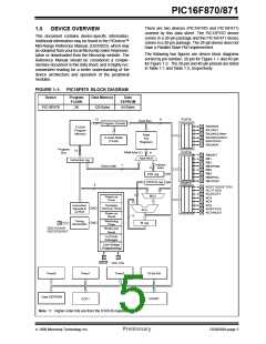
The following two figures are device block diagrams
sorted by pin number; 28-pin for Figure 1-1 and 40-pin
for Figure 1-2. The 28-pin and 40-pin pinouts are listed
in Table 1-1 and Table 1-2, respectively.
FIGURE 1-1: PIC16F870 BLOCK DIAGRAM
Device
Program
FLASH
Data Memory
Data
EEPROM
PIC16F870
2K
128 Bytes
64 Bytes
13
8
PORTA
Data Bus
Program Counter
RA0/AN0
RA1/AN1
RA2/AN2/VREF-
RA3/AN3/VREF+
RA4/T0CKI
RA5/AN4
FLASH
Program
Memory
RAM
File
Registers
8 Level Stack
(13-bit)
Program
Bus
14
RAM Addr (1)
PORTB
9
RB0/INT
RB1
RB2
RB3/PGM
RB4
Addr MUX
Instruction reg
Indirect
Addr
7
Direct Addr
8
RB5
FSR reg
RB6/PGC
RB7/PGD
STATUS reg
PORTC
8
RC0/T1OSO/T1CKI
RC1/T1OSI
RC2/CCP1
RC3
RC4
3
MUX
Power-up
Timer
Oscillator
RC5
RC6/TX/CK
RC7/RX/DT
Instruction
Decode &
Control
Start-up Timer
ALU
Power-on
Reset
8
Timing
Generation
Watchdog
Timer
W reg
OSC1/CLKIN
OSC2/CLKOUT
Brown-out
Reset
In-Circuit
Debugger
Low-Voltage
Programming
MCLR VDD, VSS
Timer2
Timer0
Timer1
CCP1
10-bit A/D
Data EEPROM
USART
Note 1: Higher order bits are from the STATUS register.
1999 Microchip Technology Inc.
Preliminary
DS30569A-page 5

 MICROCHIP [ MICROCHIP ]