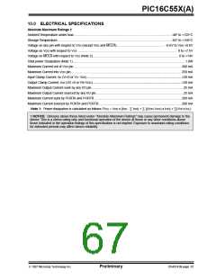
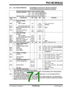
PIC16C55X(A)
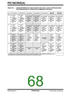
10.3
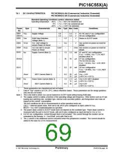
DC CHARACTERISTICS:
PIC16C55X(A) (Commercial, Industrial, Extended)
PIC16LC55X (Commercial, Industrial, Extended)
Standard Operating Conditions (unless otherwise stated)
Operating temperature –40˚C ≤ TA ≤ +85˚C for industrial and
0˚C ≤ TA ≤ +70˚C for commercial and
–40˚C ≤ TA ≤ +125˚C for automotive
Operating voltage VDD range as described in DC spec Table 10-1
Sym
Param.
No.
Characteristic
Min Typ†
Max
Unit
Conditions
VIL
Input Low Voltage
I/O ports
D030
with TTL buffer
VSS
-
-
0.8V
V
VDD = 4.5V to 5.5V
otherwise
0.15VDD
0.2VDD
0.2VDD
D031
D032
with Schmitt Trigger input
MCLR, RA4/T0CKI,OSC1 (in
RC mode)
VSS
Vss
V
V
Note1
D033
OSC1 (in XT* and HS)
OSC1 (in LP*)
Vss
Vss
-
-
0.3VDD
0.6VDD-1.0
V
V
VIH Input High Voltage
I/O ports
-
-
D040
D041
D042
D043
D043A
D070
with TTL buffer
2.0V
VDD
VDD
VDD
VDD
V
with Schmitt Trigger input 0.8VDD
MCLR RA4/T0CKI
OSC1 (XT*, HS and LP*)
OSC1 (in RC mode)
0.8VDD
0.7VDD
0.9VDD
50
-
-
V
V
Note1
IPURB PORTB weak pull-up current
200
400
µA VDD = 5.0V, VPIN = VSS
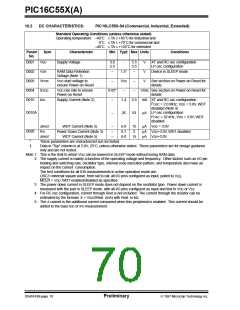
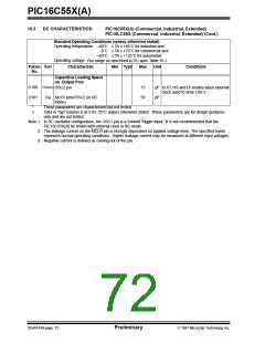
Input Leakage Current
IIL
(Notes 2, 3)
I/O ports (Except PORTA)
PORTA
RA4/T0CKI
OSC1, MCLR
±1.0
±0.5
±1.0
±5.0
µA VSS ≤ VPIN ≤ VDD, pin at hi-impedance
µA Vss ≤ VPIN ≤ VDD, pin at hi-impedance
µA Vss ≤ VPIN ≤ VDD
µA Vss ≤ VPIN ≤ VDD, XT, HS and LP osc
configuration
D060
D061
D063
-
-
-
-
-
-
VOL Output Low Voltage
D080
D083
I/O ports
-
-
-
-
-
-
-
-
0.6
0.6
0.6
0.6
V
V
V
V
IOL=8.5 mA, VDD=4.5V, -40° to +85°C
IOL=7.0 mA, VDD=4.5V, +125°C
IOL=1.6 mA, VDD=4.5V, -40° to +85°C
IOL=1.2 mA, VDD=4.5V, +125°C
OSC2/CLKOUT
(RC only)
VOH Output High Voltage (Note 3)
I/O ports (Except RA4)
D090
D092
VDD-0.7
VDD-0.7
-
-
-
-
V
V
IOH=-3.0 mA, VDD=4.5V, -40° to +85°C
IOH=-2.5 mA,
VDD=4.5V, +125°C
IOH=-1.3 mA, VDD=4.5V, -40° to +85°C
IOH=-1.0 mA,
OSC2/CLKOUT
VDD-0.7
VDD-0.7
-
-
-
-
V
V
(RC only)
VDD=4.5V, +125°C
*
VOD Open-Drain High Voltage
14*
V
RA4 pin
*
These parameters are characterized but not tested.
†
Data in “Typ” column is at 5.0V, 25°C unless otherwise stated. These parameters are for design guidance
only and are not tested.
Note 1: In RC oscillator configuration, the OSC1 pin is a Schmitt Trigger input. It is not recommended that the
PIC16C55X(A) be driven with external clock in RC mode.
2: The leakage current on the MCLR pin is strongly dependent on applied voltage level. The specified levels
represent normal operating conditions. Higher leakage current may be measured at different input voltages.
3: Negative current is defined as coming out of the pin.
1997 Microchip Technology Inc.
Preliminary
DS40143B-page 71

 MICROCHIP [ MICROCHIP ]