PIC16C55X(A)
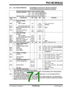
10.0 ELECTRICAL SPECIFICATIONS
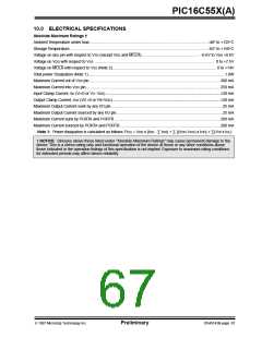
Absolute Maximum Ratings †
Ambient Temperature under bias ............................................................................................................. –40° to +125°C
Storage Temperature................................................................................................................................ –65° to +150°C
Voltage on any pin with respect to VSS (except VDD and MCLR)...................................................... –0.6V to VDD +0.6V
Voltage on VDD with respect to VSS ............................................................................................................... 0 to +7.5V
Voltage on MCLR with respect to VSS (Note 2)................................................................................................. 0 to +14V
Total power Dissipation (Note 1) ...............................................................................................................................1.0W
Maximum Current out of VSS pin...........................................................................................................................300 mA
Maximum Current into VDD pin..............................................................................................................................250 mA
Input Clamp Current, IIK (VI<0 or VI> VDD) ...................................................................................................................... ±20 mA
Output Clamp Current, IOK (V0 <0 or V0>VDD) ............................................................................................................... ±20 mA
Maximum Output Current sunk by any I/O pin ........................................................................................................25 mA
Maximum Output Current sourced by any I/O pin...................................................................................................25 mA
Maximum Current sunk by PORTA and PORTB ...................................................................................................200 mA
Maximum Current sourced by PORTA and PORTB..............................................................................................200 mA
Note 1: Power dissipation is calculated as follows: PDIS = VDD x {IDD - ∑ IOH} + ∑ {(VDD-VOH) x IOH} + ∑(VOl x IOL)
† NOTICE: Stresses above those listed under "Absolute Maximum Ratings" may cause permanent damage to the
device. This is a stress rating only and functional operation of the device at those or any other conditions above
those indicated in the operation listings of this specification is not implied. Exposure to maximum rating conditions
for extended periods may affect device reliability.
1997 Microchip Technology Inc.
Preliminary
DS40143B-page 67

 MICROCHIP [ MICROCHIP ]