PIC16F716
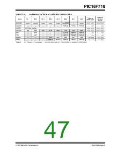
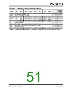
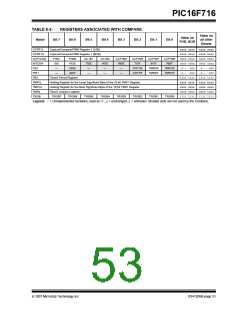
TABLE 8-2:
REGISTERS ASSOCIATED WITH CAPTURE
Value on
Value on
POR, BOR
Name
Bit 7
Bit 6
Bit 5
Bit 4
Bit 3
Bit 2
Bit 1
Bit 0
all other
Resets
CCPR1L
CCPR1H
CCP1CON
INTCON
PIE1
Capture/Compare/PWM Register 1 (LSB)
Capture/Compare/PWM Register 1 (MSB)
xxxx xxxx
xxxx xxxx
0000 0000
0000 000x
-0-- -000
-0-- -000
1111 1111
xxxx xxxx
xxxx xxxx
0000 0000
1111 1111
xxxx xxxx
xxxx xxxx
0000 0000
0000 000x
-0-- -000
-0-- -000
1111 1111
xxxx xxxx
xxxx xxxx
0000 0000
1111 1111
P1M1
GIE
—
P1M0
PEIE
ADIE
ADIF
DC1B1
T0IE
—
DC1B0
INTE
—
CCP1M3
RBIE
—
CCP1M2
T0IF
CCP1M1
INTF
CCP1M0
RBIF
CCP1IE
CCP1IF
TMR2IE
TMR2IF
TMR1IE
TMR1IF
PIR1
—
—
—
—
PR2
Timer2 Period Register
TMR1L
TMR1H
TMR2
Holding Register for the Least Significant Byte of the 16-bit TMR1 Register
Holding Register for the Most Significant Byte of the 16-bit TMR1 Register
Timer2 module’s register
TRISB
TRISB7
TRISB6
TRISB5
TRISB4
TRISB3
TRISB2
TRISB1
TRISB0
Legend: – = Unimplemented locations, read as ‘0’, u= unchanged, x= unknown. Shaded cells are not used by the Capture.
© 2007 Microchip Technology Inc.
DS41206B-page 49

 MICROCHIP [ MICROCHIP ]