PIC16F/LF1946/47
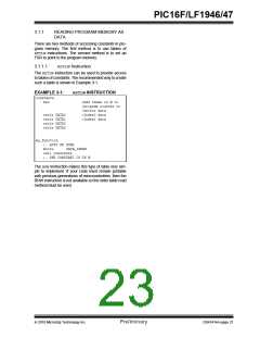
3.1.1.2
Indirect Read with FSR
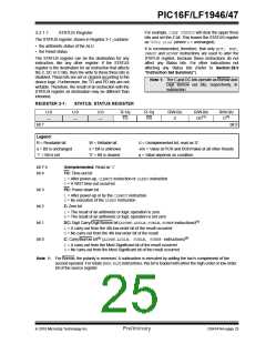
3.2.1
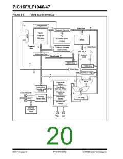
CORE REGISTERS
The program memory can be accessed as data by set-
ting bit 7 of the FSRxH register and reading the match-
ing INDFx register. The MOVIWinstruction will place the
lower 8 bits of the addressed word in the W register.
Writes to the program memory cannot be performed via
the INDF registers. Instructions that access the pro-
gram memory via the FSR require one extra instruction
cycle to complete. Example 3-2 demonstrates access-
ing the program memory via an FSR.
The core registers contain the registers that directly
affect the basic operation of the PIC16F/LF1946/47.
These registers are listed below:
• INDF0
• INDF1
• PCL
• STATUS
• FSR0 Low
• FSR0 High
• FSR1 Low
• FSR1 High
• BSR
The HIGH directive will set bit<7> if a label points to a
location in program memory.
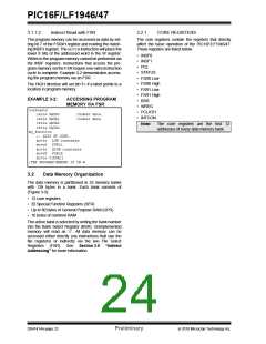
EXAMPLE 3-2:
ACCESSING PROGRAM
MEMORY VIA FSR
• WREG
constants
• PCLATH
• INTCON
retlw DATA0
retlw DATA1
retlw DATA2
retlw DATA3
my_function
;Index0 data
;Index1 data
Note:
The core registers are the first 12
addresses of every data memory bank.
;… LOTS OF CODE…
movlw
movwf
movlw
movwf
LOW constants
FSR1L
HIGH constants
FSR1H
moviw 0[FSR1]
;THE PROGRAM MEMORY IS IN W
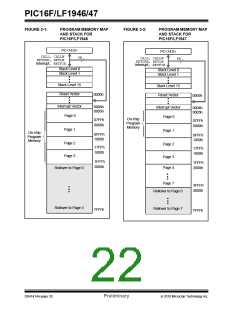
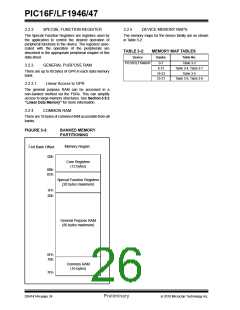
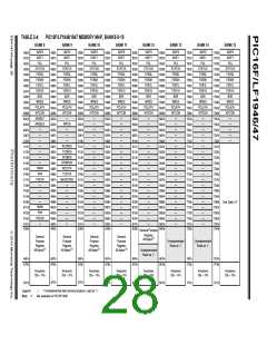
3.2
Data Memory Organization
The data memory is partitioned in 32 memory banks
with 128 bytes in a bank. Each bank consists of
(Figure 3-3):
• 12 core registers
• 20 Special Function Registers (SFR)
• Up to 80 bytes of General Purpose RAM (GPR)
• 16 bytes of common RAM
The active bank is selected by writing the bank number
into the Bank Select Register (BSR). Unimplemented
memory will read as ‘0’. All data memory can be
accessed either directly (via instructions that use the
file registers) or indirectly via the two File Select
Registers (FSR). See Section 3.5 “Indirect
Addressing” for more information.
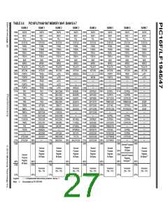
DS41414A-page 22
Preliminary
2010 Microchip Technology Inc.

 MICROCHIP [ MICROCHIP ]