PIC16F/LF1946/47
3.2.2
SPECIAL FUNCTION REGISTER
3.2.5
DEVICE MEMORY MAPS
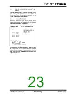
The Special Function Registers are registers used by
the application to control the desired operation of
peripheral functions in the device. The registers asso-
ciated with the operation of the peripherals are
described in the appropriate peripheral chapter of this
data sheet.
The memory maps for the device family are as shown
in Table 3-2.
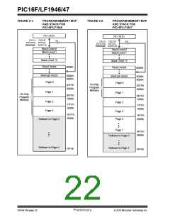
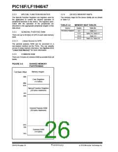
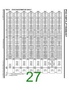
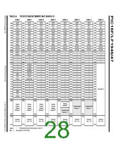
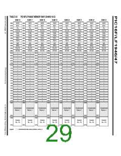
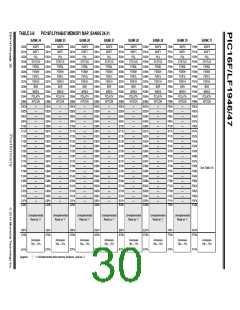
TABLE 3-2:
Device
MEMORY MAP TABLES
Banks
Table No.
PIC16F/LF1946/47
0-7
Table 3-3
Table 3-4, Table 3-7
Table 3-5
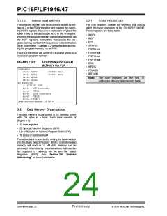
3.2.3
GENERAL PURPOSE RAM
8-15
There are up to 80 bytes of GPR in each data memory
bank.
16-23
23-31
Table 3-6, Table 3-8
3.2.3.1
Linear Access to GPR
The general purpose RAM can be accessed in a
non-banked method via the FSRs. This can simplify
access to large memory structures. See Section 3.5.2
“Linear Data Memory” for more information.
3.2.4
COMMON RAM
There are 16 bytes of common RAM accessible from all
banks.
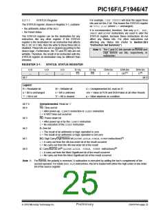
FIGURE 3-3:
BANKED MEMORY
PARTITIONING
Memory Region
7-bit Bank Offset
00h
Core Registers
(12 bytes)
0Bh
0Ch
Special Function Registers
(20 bytes maximum)
1Fh
20h
General Purpose RAM
(80 bytes maximum)
6Fh
70h
Common RAM
(16 bytes)
7Fh
DS41414A-page 24
Preliminary
2010 Microchip Technology Inc.

 MICROCHIP [ MICROCHIP ]