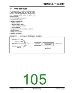
PIC16F/LF1946/47
• If the interrupt occurs during or after the execu-
tion of a SLEEPinstruction
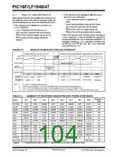
9.1.1
WAKE-UP USING INTERRUPTS
When global interrupts are disabled (GIE cleared) and
any interrupt source has both its interrupt enable bit
and interrupt flag bit set, one of the following will occur:
- SLEEPinstruction will be completely exe-
cuted
- Device will immediately wake-up from Sleep
- WDT and WDT prescaler will be cleared
- TO bit of the STATUS register will be set
- PD bit of the STATUS register will be cleared.
• If the interrupt occurs before the execution of a
SLEEPinstruction
- SLEEPinstruction will execute as a NOP.
- WDT and WDT prescaler will not be cleared
- TO bit of the STATUS register will not be set
Even if the flag bits were checked before executing a
SLEEP instruction, it may be possible for flag bits to
become set before the SLEEPinstruction completes. To
determine whether a SLEEPinstruction executed, test
the PD bit. If the PD bit is set, the SLEEP instruction
was executed as a NOP.
- PD bit of the STATUS register will not be
cleared.
FIGURE 9-1:
WAKE-UP FROM SLEEP THROUGH INTERRUPT
Q1 Q2 Q3 Q4 Q1 Q2 Q3 Q4 Q1
Q1 Q2 Q3 Q4 Q1 Q2 Q3 Q4 Q1 Q2 Q3 Q4 Q1 Q2 Q3 Q4
OSC1(1)
(3)
CLKOUT(2)
TOST
Interrupt Latency(4)
Interrupt flag
GIE bit
(INTCON reg.)
Processor in
Sleep
Instruction Flow
PC
PC
PC + 1
PC + 2
PC + 2
PC + 2
0004h
0005h
Instruction
Fetched
Inst(0004h)
Inst(PC + 1)
Inst(PC + 2)
Inst(0005h)
Inst(PC) = Sleep
Instruction
Executed
Dummy Cycle
Dummy Cycle
Sleep
Inst(PC + 1)
Inst(PC - 1)
Inst(0004h)
Note 1:
XT, HS or LP Oscillator mode assumed.
CLKOUT is not available in XT, HS or LP Oscillator modes, but shown here for timing reference.
TOST = 1024 TOSC (drawing not to scale). This delay applies only to XT, HS or LP Oscillator modes.
2:
3:
4:
GIE = 1assumed. In this case after wake-up, the processor calls the ISR at 0004h. If GIE = 0, execution will continue in-line.
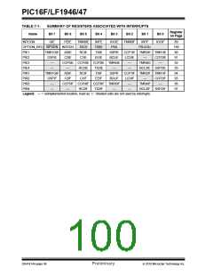
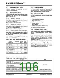
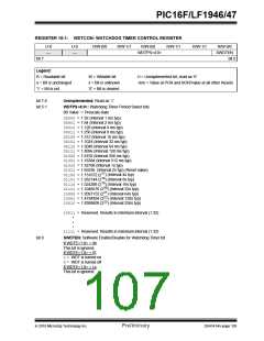
TABLE 9-1:
SUMMARY OF REGISTERS ASSOCIATED WITH POWER-DOWN MODE
Register on
Page
Name
Bit 7
Bit 6
Bit 5
Bit 4
Bit 3
Bit 2
Bit 1
Bit 0
INTCON
IOCBF
IOCBN
IOCBP
PIE1
GIE
IOCBF7
IOCBN7
IOCBP7
TMR1GIE
OSFIE
—
PEIE
IOCBF6
IOCBN6
IOCBP6
ADIE
C2IE
CCP5IE
—
TMR0IE
IOCBF5
IOCBN5
IOCBP5
RCIE
INTE
IOCBF4
IOCBN4
IOCBP4
TXIE
IOCIE
IOCBF3
IOCBN3
IOCBP3
SSPIE
BCLIE
TMR6IE
—
TMR0IF
IOCBF2
IOCBN2
IOCBP2
CCP1IE
LCDIE
—
INTF
IOCBF1
IOCBN1
IOCBP1
TMR2IE
—
IOCIF
IOCBF0
IOCBN0
IOCBP0
TMR1IE
CCP2IE
—
89
148
148
148
90
PIE2
C1IE
EEIE
91
PIE3
CCP4IE
RC2IE
RCIF
CCP3IE
TX2IE
TXIF
TMR4IE
BCL2IE
TMR2IF
—
92
PIE4
—
—
SSP2IE
TMR1IF
CCP2IF
—
93
PIR1
TMR1GIF
OSFIF
—
ADIF
C2IF
SSPIF
BCLIF
CCP1IF
LCDIF
—
94
PIR2
C1IF
EEIF
95
PIR3
CCP5IF
—
CCP4IF
RC2IF
—
CCP3IF
TX2IF
TO
TMR6IF
—
TMR4IF
BCL2IF
DC
96
PIR4
—
—
SSP2IF
C
97
STATUS
WDTCON
—
—
PD
Z
23
—
—
WDTPS<4:0>
SWDTEN
105
Legend:
— = unimplemented location, read as ‘0’. Shaded cells are not used in Power-down mode.
DS41414A-page 102
Preliminary
2010 Microchip Technology Inc.

 MICROCHIP [ MICROCHIP ]