MCP6141/2/3/4
† Notice: Stresses above those listed under “Absolute
Maximum Ratings” may cause permanent damage to the
device. This is a stress rating only and functional operation of
the device at those or any other conditions above those
indicated in the operational listings of this specification is not
implied. Exposure to maximum rating conditions for extended
periods may affect device reliability.
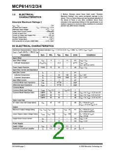
1.0
ELECTRICAL
CHARACTERISTICS
Absolute Maximum Ratings †
V
– V ........................................................................7.0V
SS
DD
All Inputs and Outputs.................... V – 0.3V to V + 0.3V
SS
DD
Difference Input voltage ...................................... |V – V
|
DD
SS
Output Short Circuit Current ..................................continuous
Current at Input Pins ....................................................±2 mA
Current at Output and Supply Pins ............................±30 mA
Storage Temperature....................................–65°C to +150°C
Junction Temperature..................................................+150°C
ESD protection on all pins (HBM; MM) ................ ≥ 4 kV; 200V
DC ELECTRICAL CHARACTERISTICS
Electrical Characteristics: Unless otherwise indicated, V = +1.4V to +5.5V, V = GND, T = 25°C, V
= V /2,
DD
SS
A
CM
DD
V
≈ V /2, and R = 1 MΩ to V /2.
DD L DD
OUT
Parameters
Sym.
Min.
Typ.
Max.
Units
Conditions
Input Offset
Input Offset Voltage
Drift with Temperature
V
-3
—
+3
—
mV
V
V
= V
SS
OS
CM
ΔV /ΔT
—
±1.5
μV/°C
= V
,
OS
A
CM
SS
T = -40°C to +125°C
A
Power Supply Rejection
PSRR
70
85
—
dB
V
= V
CM SS
Input Bias Current and Impedance
Input Bias Current
I
I
I
—
—
—
—
—
—
1
20
—
100
5000
—
pA
pA
B
B
B
Industrial Temperature
T = +85°
A
Extended Temperature
1200
1
pA
T = +125°
A
Input Offset Current
I
pA
OS
13
Common Mode Input Impedance
Differential Input Impedance
Common Mode
Z
10 ||6
—
Ω||pF
Ω||pF
CM
13
Z
10 ||6
—
DIFF
Common Mode Input Range
Common Mode Rejection Ratio
V
V
−0.3
—
80
75
80
V
+0.3
DD
V
CMR
SS
CMRR
CMRR
CMRR
62
60
60
—
dB
dB
dB
V
V
V
= 5V, V
= 5V, V
= 5V, V
= -0.3V to 5.3V
= 2.5V to 5.3V
= -0.3V to 2.5V
DD
DD
DD
CM
CM
CM
—
—
Open Loop Gain
DC Open Loop Gain (large signal)
A
95
115
—
dB
R = 50 kΩ to V /2,
OL
L
DD
V
= 0.1V to V −0.1V
OUT
DD
Output
Maximum Output Voltage Swing
V
, V
V
+ 10
—
—
V
− 10
mV
mV
R = 50 kΩ to V /2,
L DD
0.5V output overdrive
OL
OH
SS
DD
Linear Region Output Voltage Swing
Output Short Circuit Current
V
V
+ 100
V
− 100
R = 50 kΩ to V /2,
OVR
SS
DD
L
DD
A
V
V
≥ 95 dB
= 1.4V
= 5.5V
OL
I
—
—
2
—
mA
mA
SC
DD
DD
I
20
—
SC
Power Supply
Supply Voltage
V
1.4
0.3
—
5.5
1.0
V
DD
Quiescent Current per amplifier
I
0.6
μA
I
= 0
Q
O
DS21668B-page 2
© 2005 Microchip Technology Inc.

 MICROCHIP [ MICROCHIP ]