MCP414X/416X/424X/426X
7.6.1
SINGLE READ
7.6
Read Data
Normal and High Voltage
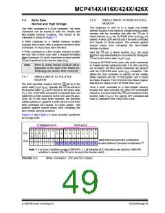
The read operation requires that the CS pin be in the
active state (VILor VIHH). Typically, the CS pin will be in
the inactive state (VIH) and is driven to the active state
(VILor VIHH). The 16-bit Read Command (Command
Byte and Data Byte) is then clocked in on the SCK and
SDI pins. The SDO pin starts driving data on the 7th bit
(CMDERR bit) and the addressed data comes out on
the 8th through 16th clocks. Figure 6-3 through
Figure 6-6 show possible waveforms for a single read.
The Read command is a 16-bit command. The Read
Command can be issued to both the Volatile and
Non-Volatile memory locations. The format of the
command is shown in Figure 7-4.
The first 6-bits of the Read command determine the
address and the command. The 7th clock will output
the CMDERR bit on the SDO pin. The remaining
9-clocks the device will transmit the 9 data bits (D8:D0)
of the specified address (AD3:AD0).
Figure 6-5 and Figure 6-6 show the single read
waveforms when the SDI and SDO signals are
multiplexed on the same pin. For additional information
on the multiplexing of these signals, refer to
Section 6.1.3 “SDI/SDO”.
Figure 7-4 shows the SDI and SDO information for a
Read command.
During a write cycle (Write or High Voltage Write to a
Non-Volatile memory location) the Read command can
only read the Volatile memory locations. By reading the
Status Register (04h), the Host Controller can
determine when the write cycle has completed (via the
state of the EEWA bit).
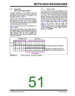
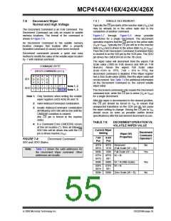
COMMAND BYTE
DATA BYTE
A
D
3
A
D
2
A
D
1
A
D
0
1
1
X
X
X
X
X
X
X
X
X
X
SDI
1
1
1
1
1
1
1
1
1
0
D
8
D
7
D
6
D
5
D
4
D
3
D
2
D
1
D Valid Address/Command combination
0
SDO
1
1
1
1
0
0
0
0
0
0
0
0
0
Attempted Non-Volatile Memory Read
during Non-Volatile Memory Write Cycle
READ DATA
Read Command - SDI and SDO States.
FIGURE 7-4:
© 2008 Microchip Technology Inc.
DS22059B-page 51

 MICROCHIP [ MICROCHIP ]