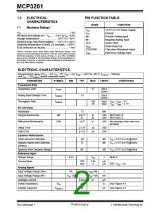
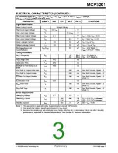
MCP3201
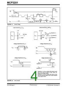
tCSH
CS
tSUCS
tHI
tLO
CLK
tEN
tDO
tDIS
tR
tF
HI-Z
HI-Z
DOUT
LSB
MSB OUT
NULL BIT
FIGURE 1-1: Serial Timing.
Load circuit for tDIS and tEN
Load circuit for tR, tF, tDO
1.4V
Test Point
VDD
t
DIS Waveform 2
EN Waveform
DIS Waveform 1
3K
Test Point
VDD/2
3K
100pF
t
DOUT
DOUT
t
CL = 100pF
VSS
Voltage Waveforms for tR, tF
Voltage Waveforms for tEN
VOH
VOL
DOUT
CS
tF
tR
1
2
3
4
CLK
DOUT
B11
tEN
Voltage Waveforms for tDO
Voltage Waveforms for tDIS
VIH
CS
DOUT
CLK
DOUT
90%
tDO
Waveform 1*
TDIS
10%
DOUT
Waveform 2†
*
Waveform 1 is for an output with internal condi-
tions such that the output is high, unless dis-
abled by the output control.
†
Waveform 2 is for an output with internal condi-
tions such that the output is low, unless disabled
by the output control.
FIGURE 1-2: Test Circuits.
DS21290B-page 4
Preliminary
1999 Microchip Technology Inc.

 MICROCHIP [ MICROCHIP ]