MCP3201
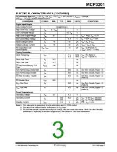
ELECTRICAL CHARACTERISTICS (CONTINUED)
All parameters apply at VDD = 5V, VSS = 0V, VREF = 5V, TAMB = -40°C to +85°C, fSAMPLE = 100ksps
and fCLK = 16*fSAMPLE unless otherwise noted.
PARAMETER
SYMBOL
MIN.
TYP.
MAX.
UNITS
CONDITIONS
Digital Input/Output
Data Coding Format
High Level Input Voltage
Straight Binary
VIH
VIL
0.7 VDD
V
V
Low Level Input Voltage
High Level Output Voltage
Low Level Output Voltage
Input Leakage Current
Output Leakage Current
0.3 VDD
VOH
4.1
V
IOH = -1mA, VDD = 4.5V
IOL = 1mA, VDD = 4.5V
VIN = VSS or VDD
VOL
0.4
10
10
10
V
ILI
-10
µA
µA
pF
ILO
-10
VOUT = VSS or VDD
Pin Capacitance (all
inputs/outputs)
CIN, COUT
VDD = 5.0V (Note 1)
TAMB = 25°C, f = 1 MHz
Timing Parameters
Clock Frequency
fCLK
1.6
0.8
MHz VDD = 5V (Note 3)
MHz VDD = 2.7V (Note 3)
Clock High Time
Clock Low Time
tHI
tLO
312
312
100
ns
ns
ns
CS Fall To First Rising CLK
Edge
tSUCS
CLK Fall To Output Data Valid
CLK Fall To Output Enable
CS Rise To Output Disable
tDO
tEN
tDIS
200
200
100
ns
ns
ns
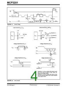
See Test Circuits, Figure 1-2
See Test Circuits, Figure 1-2
See Test Circuits, Figure 1-2
(Note 1)
CS Disable Time
tCSH
tR
625
2.7
ns
ns
DOUT Rise Time
100
100
See Test Circuits, Figure 1-2
(Note 1)
DOUT Fall Time
tF
ns
See Test Circuits, Figure 1-2
(Note 1)
Power Requirements
Operating Voltage
VDD
IDD
5.5
V
Operating Current
300
210
400
µA
µA
VDD = 5.0V, DOUT unloaded
VDD = 2.7V, DOUT unloaded
Standby Current
IDDS
0.5
2
µA
CS = VDD = 5.0V
Note 1: This parameter is guaranteed by characterization and not 100% tested.
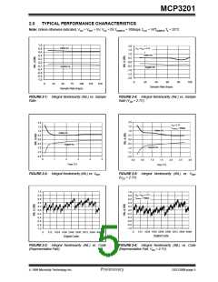
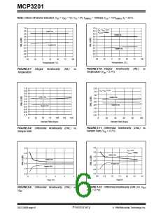
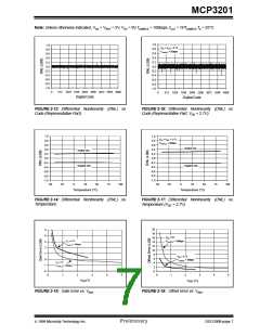
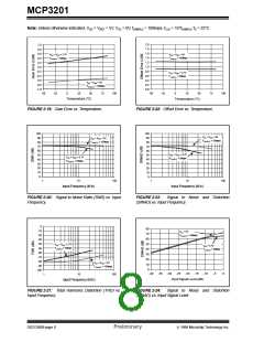
2: See graph that relates linearity performance to VREF level.
3: Because the sample cap will eventually lose charge, effective clock rates below 10kHz can affect linearity
performance, especially at elevated temperatures. See Section 6.2 for more information.
1999 Microchip Technology Inc.
Preliminary
DS21290B-page 3

 MICROCHIP [ MICROCHIP ]