MCP3201
1.0
ELECTRICAL
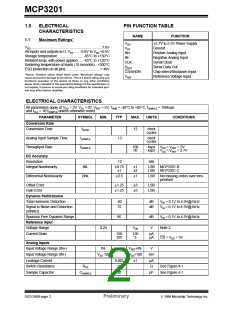
PIN FUNCTION TABLE
CHARACTERISTICS
NAME
FUNCTION
1.1
Maximum Ratings*
VDD
VSS
IN+
IN-
CLK
DOUT
CS/SHDN
VREF
+2.7V to 5.5V Power Supply
Ground
Positive Analog Input
Negative Analog Input
Serial Clock
Serial Data Out
Chip select/Shutdown Input
Reference Voltage Input
VDD.........................................................................7.0V
All inputs and outputs w.r.t. VSS ...... -0.6V to VDD +0.6V
Storage temperature ..........................-65°C to +150°C
Ambient temp. with power applied......-65°C to +125°C
Soldering temperature of leads (10 seconds) ..+300°C
ESD protection on all pins...................................> 4kV
*Notice: Stresses above those listed under “Maximum ratings” may
cause permanent damage to the device. This is a stress rating only and
functional operation of the device at those or any other conditions
above those indicated in the operational listings of this specification is
not implied. Exposure to maximum rating conditions for extended peri-
ods may affect device reliability.
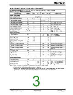
ELECTRICAL CHARACTERISTICS
All parameters apply at VDD = 5V, VSS = 0V, VREF = 5V, TAMB = -40°C to +85°C, fSAMPLE = 100ksps
and fCLK = 16*fSAMPLE unless otherwise noted.
PARAMETER
Conversion Rate
SYMBOL
MIN.
TYP.
MAX.
UNITS
CONDITIONS
Conversion Time
tCONV
12
clock
cycles
Analog Input Sample Time
Throughput Rate
tSAMPLE
fSAMPLE
1.5
clock
cycles
100
50
ksps VDD = VREF = 5V
ksps VDD = VREF = 2.7V
DC Accuracy
Resolution
12
bits
Integral Nonlinearity
INL
±0.75
±1
±1
±2
LSB
LSB
MCP3201-B
MCP3201-C
Differential Nonlinearity
DNL
±0.5
±1
LSB
No missing codes over tem-
perature
Offset Error
±1.25
±1.25
±3
±5
LSB
LSB
Gain Error
Dynamic Performance
Total Harmonic Distortion
-82
72
dB
dB
VIN = 0.1V to 4.9V@1kHz
VIN = 0.1V to 4.9V@1kHz
Signal to Noise and Distortion
(SINAD)
Spurious Free Dynamic Range
Reference Input
86
dB
VIN = 0.1V to 4.9V@1kHz
Voltage Range
0.25
VDD
V
Note 2
Current Drain
100
.001
150
3
µA
µA
CS = VDD = 5V
Analog Inputs
Input Voltage Range (IN+)
IN-
VREF+IN-
V
Input Voltage Range (IN-)
VSS-100
VSS+100
±1
mV
Leakage Current
Switch Resistance
0.001
1K
µA
RSS
Ω
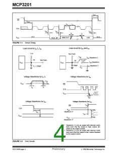
See Figure 4-1
See Figure 4-1
Sample Capacitor
CSAMPLE
20
pF
DS21290B-page 2
Preliminary
1999 Microchip Technology Inc.

 MICROCHIP [ MICROCHIP ]