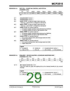
MCP2515
4.4.3
CONFIGURED AS DIGITAL OUTPUT
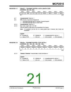
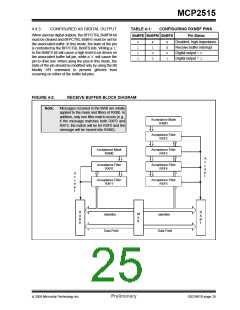
TABLE 4-1:
CONFIGURING RXNBF PINS
When used as digital outputs, the BFPCTRL.BxBFM bit
must be cleared and BFPCTRL.BnBFE must be set for
the associated buffer. In this mode, the state of the pin
is controlled by the BFPCTRL.BnBFS bits. Writing a ‘1’
to the BnBFS bit will cause a high level to be driven on
the associated buffer full pin, while a ‘0’ will cause the
pin to drive low. When using the pins in this mode, the
state of the pin should be modified only by using the Bit
Modify SPI command to prevent glitches from
occurring on either of the buffer full pins.
BnBFE BnBFM BnBFS
Pin Status
0
1
1
1
X
1
0
0
X
X
0
1
Disabled, high-impedance
Receive buffer interrupt
Digital output = 0
Digital output = 1
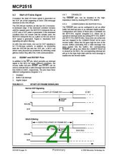
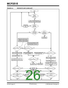
FIGURE 4-2:
Note:
RECEIVE BUFFER BLOCK DIAGRAM
Messages received in the MAB are intially
applied to the mask and filters of RXB0. In
addition, only one filter match occurs (e.g.,
if the message matches both RXF0 and
RXF2, the match will be for RXF0 and the
message will be moved into RXB0).
Acceptance Mask
RXM1
Acceptance Filter
RXF2
Acceptance Mask
RXM0
Acceptance Filter
RXF3
A
c
c
e
p
t
Acceptance Filter
RXF0
Acceptance Filter
RXF4
A
c
Acceptance Filter
RXF1
Acceptance Filter
RXF5
c
e
p
t
R
X
B
0
R
X
B
1
M
A
B
Identifier
Identifier
Data Field
Data Field
© 2005 Microchip Technology Inc.
Preliminary
DS21801D-page 25

 MICROCHIP [ MICROCHIP ]