MCP201
1.5.3
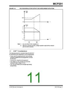
POWER OUTPUT (VREG)
1.5
Pin Descriptions
Positive Supply Voltage Regulator Output pin.
TABLE 1-3:
Devices
MCP201 PINOUT OVERVIEW
1.5.4
TRANSMIT DATA INPUT (TXD)
Function
Bond Pad
The Transmit Data Input pin has an internal pull-up to
VREG. The LIN pin is low (dominant) when TXD is low,
and high (recessive) when TXD is high.
8-Pin PDIP/
SOIC/DFN
Name
Normal Operation
1
RXD
Receive Data Output
(CMOS output)
In case the thermal protection detects an over-temper-
ature condition while the signal TXD is low, the
transmitter is shutdown. The recovery from the thermal
shutdown is equal to adequate cooling time.
2
CS/WAKE
Chip Select (TTL-HV
input)
3
4
VREG
TXD
Power Output
1.5.5
GROUND (VSS)
Transmit Data Input
(TTL)
Ground pin.
5
6
VSS
LIN
Ground
1.5.6
LIN
LIN bus (bidirectional-
HV)
The bidirectional LIN bus Interface pin is the driver unit
for the LIN pin and is controlled by the signal TXD. LIN
has an open collector output with a current limitation.
To reduce EMI, the edges during the signal changes
are slope-controlled.
7
8
VBAT
Battery
FAULT/SLPS Fault Detect Output,
Slope Select Input
Legend: TTL = TTL input buffer,
1.5.7
BATTERY (VBAT)
HV = High Voltage (VBAT)
Battery Positive Supply Voltage pin. This pin is also the
input for the internal voltage regulator.
1.5.1
RECEIVE DATA OUTPUT (RXD)
The Receive Data Output pin is a standard CMOS
output and follows the state of the LIN pin.
1.5.8
FAULT/SLPS
FAULT Detect Output, Slope Select Input.
The LIN receiver monitors the state of the LIN pin and
generates the output signal RXD.
This pin is usually in Output mode. Its state is defined
as shown in Table 1-5.
1.5.2
CS/WAKE
The state of this pin is internally sampled during power-
on of VBAT. Once VBAT has reached a stable level,
(approximately 6 VDC) and VREG is stable at 4.75 to
5.25 VDC, the state of this pin selects which slew rate
profile to apply to the LIN output. It is only during this
time that the pin is used as an input (the output driver
is off during this time). The slope will stay selected until
the next VBAT power-off/power-on sequence, regard-
less of any power-down, wake-up or SLEEP events.
Only a VBAT rising state will cause a sampling of the
FAULT/SLPS pin. The Slope selection will be made
irrespective of the state of any other pin.
Chip Select Input pin. This pin controls whether the part
goes into READY1 or READY mode at power-up. The
internal pull-down resistor will keep the CS/WAKE pin
low. This is done to ensure that no disruptive data will
be present on the bus while the microcontroller is
executing a Power-on Reset and I/O initialization
sequence. The pin must see a low-to-high transition to
activate the transmitter.
After CS/WAKE transitions to ‘1’, the transmitter is
enabled. If CS/WAKE = ‘0’, the device is in Ready1
mode on power-up or in Low-Power mode. In Low-
Power mode, the voltage regulator is shut down, the
transmitter driver is disabled and the receiver logic is
enabled.
The FAULT/SLPS pin is connected to either VREG or
VSS through a resistor (approximately 100 kΩ) to make
the slope selection. This large resistance allows the
FAULT indication function to overdrive the resistor in
normal operation mode.
An external switch (see Figure 1-2) can then wake up
both the transceiver and the microcontroller. An
external-blocking diode and current-limiting resistor are
necessary to protect the microcontroller I/O pin.
If the FAULT/SLPS is high (‘1’), the normal slope shap-
ing is selected (dv/dt = 2 V/µs). If FAULT/SLPS is low
(‘0’) during this time, the alternate slope-shaping is
selected (dv/dt = 4 V/µs). This mode can be used if a
user desires to run at a faster slope. This mode is not
LIN compliant.
Note:
On POR, the MCP201 enters Ready or
Ready1 mode (see Figure 1-1). In order to
enter Operational mode, the MCP201 has
to see one rising edge on CS/WAKE
600 µs after the voltage regulator reaches
5V.
© 2007 Microchip Technology Inc.
DS21730F-page 7

 MICROCHIP [ MICROCHIP ]