MCP201
1.4
Typical Applications
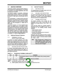
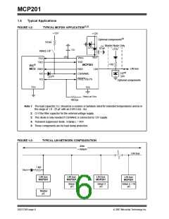
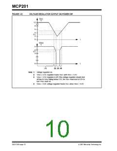
FIGURE 1-2:
TYPICAL MCP201 APPLICATION(1,2)
+12V
+12V
Optional components(5)
10 kΩ
Master Node Only
CF
27V
10 uF
+12V
CG
WAKE-UP
+5V
VBAT
VREG
TXD
VDD
TXD
1 kΩ
PIC®
MCP201
LIN bus
MCU
RXD
I/O
RXD
LIN
D2(4)
24V
CS/WAKE
D1(3)
I/O
FAULT/SLPS
VSS
Optional components
VSS
VREG or VSS
100 kΩ
Note 1: The load capacitor, CG, should be a ceramic or tantalum rated for extended temperatures and be in
the range of 1.0 - 22 µF with an ESR 0.4Ω - 5Ω.
2: CF if the filter capacitor for the external voltage supply.
3: This diode is only needed if CS/WAKE is connected to 12V supply.
4: Transient suppressor diode. Vclamp L = 40V.
5: These components are for load dump protection.
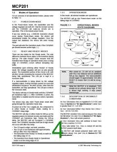
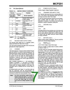
FIGURE 1-3:
TYPICAL LIN NETWORK CONFIGURATION
40m
+ Return
LIN bus
1 kΩ
VBAT
LIN bus
MCP201
LIN bus
MCP201
LIN bus
MCP201
LIN bus
MCP201
Slave 1
µC
Slave 2
µC
Slave n <16
µC
Master
µC
DS21730F-page 6
© 2007 Microchip Technology Inc.

 MICROCHIP [ MICROCHIP ]