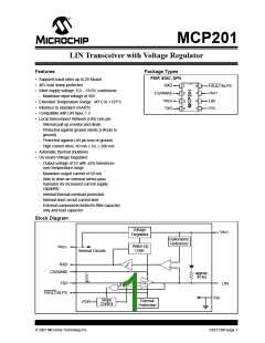
MCP201
1.3.3
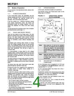
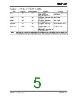
OPERATION MODE
1.3
Modes of Operation
In this mode, all internal modules are operational.
For an overview of all operational modes, please refer
to Table 1-2.
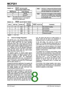
The MCP201 will go into Power-down mode on the
falling edge of CS/WAKE.
1.3.1
POWER-DOWN MODE
In the Power-down mode, the transmitter and the
voltage regulator are both off. Only the receiver section
and the CS/WAKE pin wake-up circuits are in
operation. This is the lowest power mode.
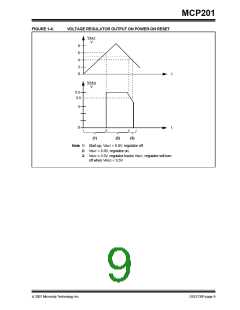
FIGURE 1-1:
OPERATIONAL MODES
STATE DIAGRAMS
CS/WAKE = true
Power-down
Mode
If any bus activity (e.g., a BREAK character) should
occur during Power-down mode, the device will
immediately enable the voltage regulator. Once the
output has stabilized, the device will enter Ready
mode.
Bus Activity
CS/WAKE = false
Operation
Mode
Ready
Mode
The part will enter the Operation mode, if the CS/WAKE
pin should become active-high (‘1’).
1.3.2
READY AND READY1 MODES
POR
Start
CS/WAKE = true
There are two states for the Ready mode. The only
difference between these states is the transition during
start-up. The state Ready1 mode ensures that the
transition from Ready to Operation mode (once a rising
edge of CS/WAKE) occurs without disrupting bus
traffic.
CS/WAKE = false
CS/WAKE = true
Ready1
Mode
Immediately upon entering either Ready1 or Ready
mode, the voltage regulator will turn on and provide
power. The transmitter portion of the circuit is off, with
all other circuits (including the receiver) of the MCP201
being fully operational. The LIN pin is kept in a
recessive state.
Note:
Note:
After power-on, CS will not be sampled
until VREG has stabized and an additional
600 µs has elapsed. The microcontroller
should toggle CS approximately 1mS after
RESET to ensure that CS will be recog-
nized.
If a microcontroller is being driven by the voltage
regulator output, it will go through a power-on reset and
initialization sequence. All other circuits, other than the
transmitter, are fully operational. The LIN pin is held in
the recessive state.
While the MCP201 is in shutdown, TXD
should not be actively driven high. If TXD
is driven high actively, it may power
internal logic.
The device will stay in Ready mode until the CS/WAKE
pin transitions high (‘1’). After CS/WAKE is active, the
transmitter is enabled and the device enters Operation
mode.
1.3.4
DESCRIPTION OF BROWNOUT
CONDITIONS
As VBAT decreases VREG is regulated to 5.0 VDC (see
VREG in Section 2.2 “DC Specifications”) while VBAT
is greater than 5.5 - 6.0 VDC.
The device may only enter Power-down mode after
going through the Operation mode step.
At power-on of the VBAT supply pin, the component is
in either Ready or Ready1 mode, waiting for a
CS/WAKE rising edge.
As VBAT decreases further VREG tracks VBAT (VREG =
VBAT - (0.5 to 1.0) VDC.
The MCP201 monitors VREG and as long as VREG does
not fall below VSD (see VSD in Section 2.2 “DC Spec-
ifications”), VREG will remain powered.
The MCP201 will stay in either mode for 600 µs as the
regulator powers its internal circuitry and waits until the
CS/WAKE pin transitions high. During the 600 µs
delay, the MCP201 will not recognize a CS/WAKE
event. The CS/WAKE transition from low to high should
not occur until after this delay.
As VBAT increases VREG will continue to track VBAT
until VREG reaches 5.0 VDC.
If VREG falls below VSD, VREG is turned off and the
MCP201 powers itself down.
• The CS input is edge, not level, sensitive.
• The CS pin is not monitored until approximately
600 µs after VREG has stabized.
• The transistion from Ready1 to Ready is made on
the falling edge of CS.
The MCP201 will remain powered down until VBAT
increases above VON (see VON in Section 2.2 “DC
Specifications”.
• The transition from Ready mode to Operational
mode is on the rising edge of CS.
DS21730F-page 4
© 2007 Microchip Technology Inc.

 MICROCHIP [ MICROCHIP ]