24LC04B/08B
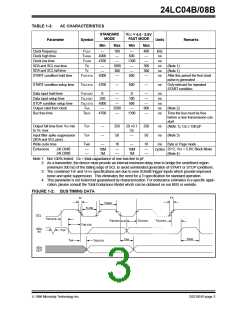
FIGURE 7-1: CURRENT ADDRESS READ
S
T
S
T
A
R
T
BUS ACTIVITY
MASTER
CONTROL
BYTE
O
DATA n
P
SDA LINE
S
P
A
C
K
N
O
BUS ACTIVITY
A
C
K
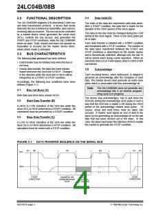
FIGURE 7-2: RANDOM READ
S
T
O
P
S
T
A
R
T
S
T
A
R
T
BUS ACTIVITY
MASTER
CONTROL
BYTE
WORD
ADDRESS (n)
CONTROL
BYTE
DATA (n)
S
P
S
SDA LINE
A
C
K
A
C
K
A
C
K
N
O
BUS ACTIVITY
A
C
K
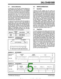
FIGURE 7-3: SEQUENTIAL READ
S
T
O
P
BUS ACTIVITY
MASTER
CONTROL
BYTE
DATA n
DATA n + 1
DATA n + 2
DATA n + X
SDA LINE
P
A
C
K
A
C
K
A
C
K
A
C
K
N
O
BUS ACTIVITY
A
C
K
8.3
WP
8.0
PIN DESCRIPTIONS
This pin must be connected to either VSS or VCC.
8.1
SDA Serial Address/Data Input/Output
If tied to VSS, normal memory operation is enabled
(read/write the entire memory).
This is a Bi-directional pin used to transfer addresses
and data into and data out of the device. It is an open
drain terminal, therefore the SDA bus requires a pullup
resistor to VCC (typical 10KΩ for 100 kHz, 1KΩ for 400
kHz).
If tied to VCC, WRITE operations are inhibited. The
entire memory will be write-protected. Read operations
are not affected.
This feature allows the user to use the 24LC04B/08B as
a serial ROM when WP is enabled (tied to VCC).
For normal data transfer SDA is allowed to change only
during SCL low. Changes during SCL high are
reserved for indicating the START and STOP condi-
tions.
8.4
A0, A1, A2
These pins are not used by the 24LC04B/08B. They
may be left floating or tied to either VSS or VCC.
8.2
SCL Serial Clock
This input is used to synchronize the data transfer from
and to the device.
1996 Microchip Technology Inc.
DS21051E-page 7

 MICROCHIP [ MICROCHIP ]