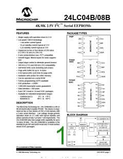
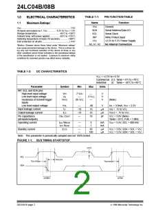
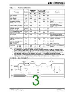
24LC04B/08B
3.6
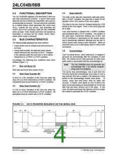
Device Addressing
4.0
WRITE OPERATION
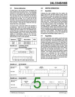
A control byte is the first byte received following the
start condition from the master device. The control byte
consists of a 4-bit control code, for the 24LC04B/08B
this is set as 1010 binary for read and write operations.
The next three bits of the control byte are the block
select bits (B2, B1, B0). B2 is a don't care for both the
24LC04B and 24LC08B; B1 is a don't care for the
24LC04B. They are used by the master device to select
which of the two or four 256 word blocks of memory are
to be accessed. These bits are in effect the most sig-
nificant bits of the word address.
4.1
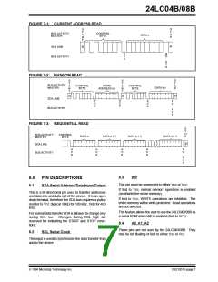
Byte Write
Following the start condition from the master, the
device code (4 bits), the block address (3 bits), and the
R/W bit which is a logic low is placed onto the bus by
the master transmitter. This indicates to the addressed
slave receiver that a byte with a word address will follow
after it has generated an acknowledge bit during the
ninth clock cycle. Therefore the next byte transmitted
by the master is the word address and will be written
into the address pointer of the 24LC04B/08B. After
receiving another acknowledge signal from the
24LC04B/08B the master device will transmit the data
word to be written into the addressed memory location.
The 24LC04B/08B acknowledges again and the master
generates a stop condition. This initiates the internal
write cycle, and during this time the 24LC04B/08B will
not generate acknowledge signals (Figure 4-1).
The last bit of the control byte defines the operation to
be performed. When set to one a read operation is
selected, when set to zero a write operation is selected.
Following the start condition, the 24LC04B/08B moni-
tors the SDA bus checking the device type identifier
being transmitted, upon a 1010 code the slave device
outputs an acknowledge signal on the SDA line.
Depending on the state of the R/W bit, the 24LC04B/
08B will select a read or write operation.
4.2
Page Write
The write control byte, word address and the first data
byte are transmitted to the 24LC04B/08B in the same
way as in a byte write. But instead of generating a stop
condition the master transmits up to 16 data bytes to
the 24LC04B/08B which are temporarily stored in the
on-chip page buffer and will be written into the memory
after the master has transmitted a stop condition. After
the receipt of each word, the four lower order address
pointer bits are internally incremented by one. The
higher order seven bits of the word address remains
constant. If the master should transmit more than 16
words prior to generating the stop condition, the
address counter will roll over and the previously
received data will be overwritten. As with the byte write
operation, once the stop condition is received an inter-
nal write cycle will begin (Figure 4-2).
Control
Code
Operation
Block Select
R/W
Read
Write
1010
1010
Block Address
Block Address
1
0
FIGURE 3-2: CONTROL BYTE
ALLOCATION
START
READ/WRITE
SLAVE ADDRESS
R/W A
1
0
1
0
X
B1
B0
X = Don’t care. B1 is don’t care for 24LC04B.
FIGURE 4-1: BYTE WRITE
S
T
A
R
T
S
BUS ACTIVITY
MASTER
CONTROL
BYTE
WORD
ADDRESS
T
DATA
O
P
SDA LINE
S
P
A
C
K
A
C
K
A
C
K
BUS ACTIVITY
FIGURE 4-2: PAGE WRITE
S
BUS ACTIVITY
MASTER
T
A
R
T
S
T
O
P
CONTROL
BYTE
WORD
ADDRESS (n)
DATA n
DATA n + 1
DATA n + 15
SDA LINE
S
P
A
C
K
A
C
K
A
C
K
A
C
K
A
C
K
BUS ACTIVITY
1996 Microchip Technology Inc.
DS21051E-page 5
This document was created with FrameMaker 4 0 4

 MICROCHIP [ MICROCHIP ]