MIC4423/4424/4425
Micrel
in estimating power dissipation in the driver. Operating on resistance of the driver when its output is in the high state,
frequency, power supply voltage, and load all affect power or its on resistance when the driver is in the low state,
dissipation.
depending on how the inductor is connected, and this is still
only half the story. For the part of the cycle when the inductor
is forcing current through the driver, dissipation is best
described as
Given the power dissipation in the device, and the thermal
resistance of the package, junction operating temperature for
any ambient is easy to calculate. For example, the thermal
resistanceofthe8-pinplasticDIPpackage,fromthedatasheet,
is 150°C/W. In a 25°C ambient, then, using a maximum
junction temperature of 150°C, this package will dissipate
960mW.
P
L2
= I V (1 – D)
D
where V is the forward drop of the clamp diode in the driver
D
(generally around 0.7V). The two parts of the load dissipation
must be summed in to produce P
L
Accurate power dissipation numbers can be obtained by
summingthethreesourcesofpowerdissipationinthedevice:
P = P + P
L2
L
L1
Quiescent Power Dissipation
• Load power dissipation (P )
• Quiescent power dissipation (P )
L
Quiescent power dissipation (P , as described in the input
Q
Q
section) depends on whether the input is high or low. A low
input will result in a maximum current drain (per driver) of
≤0.2mA; a logic high will result in a current drain of ≤2.0mA.
Quiescent power can therefore be found from:
• Transition power dissipation (P )
T
Calculation of load power dissipation differs depending on
whether the load is capacitive, resistive or inductive.
Resistive Load Power Dissipation
P = V [D I + (1 – D) I ]
Q
S
H
L
Dissipation caused by a resistive load can be calculated as:
2
where:
P = I R D
L
O
I = quiescent current with input high
H
where:
I = quiescent current with input low
L
D = fraction of time input is high (duty cycle)
V = power supply voltage
S
I = the current drawn by the load
R
= the output resistance of the driver when the
output is high, at the power supply voltage used
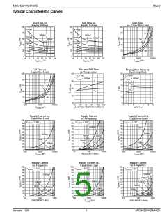
(See characteristic curves)
O
Transition Power Dissipation
Transitionpowerisdissipatedinthedrivereachtimeitsoutput
changes state, because during the transition, for a very brief
interval, both the N- and P-channel MOSFETs in the output
totem-poleareONsimultaneously,andacurrentisconducted
D = fraction of time the load is conducting (duty cycle)
Capacitive Load Power Dissipation
Dissipation caused by a capacitive load is simply the energy
placedin,orremovedfrom,theloadcapacitancebythedriver.
The energy stored in a capacitor is described by the equation:
through them from V to ground. The transition power
S
dissipation is approximately:
P = f V (A•s)
T
S
2
E = 1/2 C V
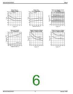
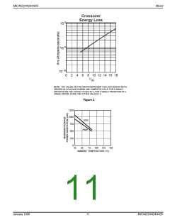
where (A•s) is a time-current factor derived from Figure 2.
Asthisenergyislostinthedrivereachtimetheloadischarged
or discharged, for power dissipation calculations the 1/2 is Total power (PD) then, as previously described is just
removed. This equation also shows that it is good practice not
P = P + P +P
T
D
L
Q
to place more voltage in the capacitor than is necessary, as
dissipation increases as the square of the voltage applied to
the capacitor. For a driver with a capacitive load:
Examples show the relative magnitude for each term.
EXAMPLE 1: A MIC4423 operating on a 12V supply driving
two capacitive loads of 3000pF each, operating at 250kHz,
with a duty cycle of 50%, in a maximum ambient of 60°C.
2
P = f C (V )
L
S
where:
First calculate load power loss:
2
f = Operating Frequency
C = Load Capacitance
V = Driver Supply Voltage
S
P = f x C x (V )
L
S
–9
–9
2
P = 250,000 x (3 x 10 + 3 x 10 ) x 12
L
= 0.2160W
Inductive Load Power Dissipation
Then transition power loss:
P = f x V x (A•s)
For inductive loads the situation is more complicated. For the
part of the cycle in which the driver is actively forcing current
into the inductor, the situation is the same as it is in the
resistive case:
T
S
–9
= 250,000 • 12 • 2.2 x 10 = 6.6mW
Then quiescent power loss:
= V x [D x I + (1 – D) x I ]
2
P
L1
= I R
D
O
P
Q
S
H
L
However, in this instance the R required may be either the
O
January 1999
9
MIC4423/4424/4425

 MICREL [ MICREL SEMICONDUCTOR ]