MIC2042/2043
Micrel
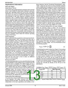
Figure 4. Lower UVLO Setting
Power Dissipation
heatupconsiderably. Thefollowinglistcontainssomeuseful
suggestions for PCB layout design of the MIC2042/43 in
order to prevent the die from overheating under normal
operating conditions:
Power dissipation depends on several factors such as the
load, PCB layout, ambient temperature, and package type.
The following equations can be used to calculate power
dissipation and die temperature.
1. Supply additional copper area under the device
to remove heat away from the IC.
Calculation of power dissipation can be accomplished by the
following equation:
2
See “Application Hint 17” for a general guideline
in calculating the suggested area.
P = R
× (I )
OUT
(5)
D
DS(ON)
To relate this to junction temperature, the following equation
can be used:
2. Provide additional pad area on the corner pins of
the MIC2042/43 IC for heat distribution.
T = P × Rθ + T
(6)
where T = junction temperature, T = ambient temperature
J
D
JA
A
3. Tie the common power pins (VIN = pins 8 and
12 and VOUT = pins 10, 11, 14 for the 14-pin
TSSOP, VIN = pins 5 and 7 and VOUT = pins 6
and 8 for the 8-pin SOP) together in a manner
such that the traces entering and leaving the
device have a uniform width sufficient for the
application’s current requirements plus added
margin (25% minimum recommended).
J
A
and Rθ is the thermal resistance of the package.
JA
Printed Circuit Board Hot-Plug
The MIC2042/43 are ideal inrush current limiting power
switches suitable for hot-plug applications. Due to the inte-
grated charge pump, the MIC2042/43 present a high imped-
ance when in the off state and the device slowly becomes a
low impedance as it turns on. This effectively isolates power
supplies from highly capacitive loads by reducing inrush
currentduringhot-plugevents.Thissamefeaturealsocanbe
used for soft-start requirements.
Ex: For 2A maximum current, design traces for
2.5A capability.
4. For PCB trace width calculation, there are
numerous calculator programs available on the
internet and elsewhere. As a general rule of
thumb, 15-20 mils for every 1A of current when
using 1oz. copper. However, the trace width
calculators often take into account maximum
temperature increase constraints, as well as
layer arrangement, in determining the PCB trace
widths.
PCB Layout Recommendations
The MIC2042 and MIC2043 have very low on-resistance,
typically 40mΩ, and the switches can provide up to 3A of
continuous output current. Under such heavy loads, the
power consumed by the devices may cause the devices to
M0512-112603
14
January 2005

 MICREL [ MICREL SEMICONDUCTOR ]