MIC2042/2043
Micrel
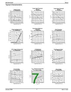
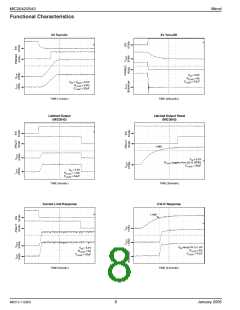
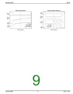
linear response. See the “Functional Characteristics” plots.
Table 1 shows the rise time for various standard capacitor
values.Additionally,theoutputturn-ontimemustbelessthan
the nominal flag delay of 28ms in order to avoid nuisance
tripping of the /FAULT output. This limit is imposed by the
current limiting circuitry which monitors the (VIN – VOUT)
differential voltage and concludes a fault condition is present
if the differential voltage exceeds 200mV for more than the
flag delay period. For the MIC2043, the /FAULT will assert
and the output will latch off if the output is not within 200mV
of the input before the flag delay times out. When using the
active-low (–2) option with the EN input tied to ground, slew
control is functional during initial start-up but does not func-
tion upon resetting the input power to the device. In order for
the SLEW control to operate during consecutive system
restarts, the EN pin must reset (toggle OFF to ON).
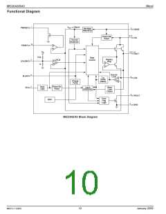
Applications Information
Input and Output
Supply Bypass Filtering
The need for input supply bypass is necessary due to several
factors, most notably the input/output inductance along the
power path, operating current and current limit, and output
capacitance. A 0.1µF to 0.47µF bypass capacitor positioned
very close to the VIN pin to GND of the device is strongly
recommended to filter high frequency oscillations due to
inductance. Also, a sufficient bypass capacitor positioned
close to the input source to the switch is strongly advised in
order to suppress supply transient spikes and to limit input
voltage droop. Inrush current increases with larger output
capacitance, thus the minimum value of this capacitor will
require experimental determination for the intended applica-
tion and design. A good starting point is a capacitor between
4.7µF to 15µF. Without these bypass capacitors, an extreme
overload condition such as a short circuit, or a large capaci-
tive load, may cause either the input supply to exceed the
maximum rating of 6V and possibly cause damage to the
internal control circuitry or allow the input supply to droop and
fall out of regulation and/or below the minimum operating
voltage of the device.
UVLO Threshold Setting With Low Input Voltages
When the switching voltage is below 1.6V, the device’s
standard UVLO threshold (1.45V nominal) will hinder the
output MOSFET in switching VIN to VOUT. In this case, the
use of the UVLOIN pin is required to override the standard
UVLO threshold and set a new, lower threshold for the lower
input voltage. An external resistive divider network con-
nected at the UVLOIN pin is used to set the new threshold.
Due to the ratio of the internal components, the total series
resistance of the external resistive divider should not exceed
200kΩ.ThecircuitshowninFigure4illustratesanapplication
that switches 0.8V while the device is powered from a
separate 2.5V power supply. The UVLO threshold is set by
the following equation:
Output Capacitance
WhentheMIC2042dieexceedstheovertemperaturethresh-
old of approximately 140°C, the device can enter into a
thermal shutdown mode if the die temperature falls below
120°C and then rises above 140°C in a continuous cycle.
With the VOUT and /FAULT outputs cycling on and off, the
MIC2042 will reset the /FAULT while in an overtemperature
fault condition if the output voltage is allowed to swing below
ground. The inductance present at the output must be neu-
tralizedbycapacitanceinordertoensurethattheoutputdoes
not fall below ground. In order to counter the board parasitic
inductance and the inductance of relatively short-length
power cable (≤ 1ft., 16 to 20 gauge wire), a minimum output
capacitanceof22µFisstronglyrecommendedandshouldbe
placed close to the VOUT pin of the MIC2042. For applica-
tions that use more than a foot of cable, an additional
10µF/ft. is recommended.
R2
R3
V
= 0.23V × 1+
(4)
UVTH
In substituting the resistor values from Figure 4, the resulting
UVLO threshold (V ) is calculated as 0.6V for this 0.8V
UVTH
switching application. When using the UVLOIN pin to set a
new UVLO threshold, an optional 0.1µF to 1.0µF capacitor
from UVLOIN to GND may be used as a glitch filter in order
to avoid nuisance tripping of the UVLO threshold. If the
UVLOIN pin is not in use, this pin should be left open
(floating). The use of a pull-down resistor to ground will offset
the ratio of the internal resistive divider to this pin resulting in
a shift in the UVLO threshold. To bypass (disable) UVLO,
connect the UVLOIN pin directly to the VIN pin of the
MIC2042/43.
Reverse Current Block
The MIC2042/43 provides reverse current flow block through
theoutputMOSFETifthevoltageatVOUTisgreaterthanVIN
when the device is disabled. The VBIAS supply pin has a
limited reverse current flow if the voltage at VOUT is pulled
above VBIAS when the device is disabled. A graph of the
V
= V
= 5V/3V; C
= 47µF; I = 1A
LOAD
Conditions:
IN
BIAS
LOAD
V
reverse current flow is shown in the “Functional Char-
BIAS
acteristics” plots. The reverse current for V
can be
C
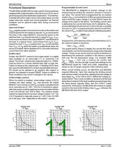
(µF)
Rise Time (ms)
BIAS
SLEW
completely blocked by inserting a Schottky diode from the
VBIAS pin (cathode) to the supply (anode). However, the
minimum voltage of 1.6V must be supplied to VBIAS after
accounting for the voltage drop across the diode.
5V
3
3V
4.75
15
0.01
0.033
0.047
0.1
10.5
14
21
Output Slew-Rate Adjustment
32
46
Theoutputslew-ratefortheMIC2042/43canbesloweddown
by the capacitor (16V rating, minimum; 25V suggested)
between SLEW and GND. The slew-rate control circuitry is
independent of the load capacitance and exhibits a non-
Table 1. Typical Output Rise Time for Various C
SLEW
January 2005
13
M0512-112603

 MICREL [ MICREL SEMICONDUCTOR ]