MIC2042/2043
Micrel
Programmable Current Limit
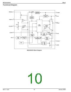
Functional Description
The MIC2042/43 is designed to prevent damage to the
external load by limiting the maximum amount of current it
can draw. The current limit is programmed by an external
TheMIC2042andMIC2043arehigh-sideN-Channelswitches
equipped with programmable current limit up to 3A for use in
generalpurposepowerdistributionapplications.Theswitches,
availablewithactive-highoractive-lowenableinputs,provide
output slew-rate control and circuit protection via thermal
shutdown and an optional output latch during overcurrent
conditions.
resistor (R
) connected from ILIM to ground and becomes
SET
active when the output voltage is at least 200mV below the
voltage at the input to the device. The limiting current value
is defined by the current limit factor (CLF) divided by R
and the MIC2042/43 will limit from 0.5A to 3A with a set point
,
SET
Input and Output
accuracy of ±22%. In programming the nominal current limit,
V
suppliespowertotheinternalcircuitryoftheswitchand
the value of R
is determined using the following equation:
BIAS
SET
must be present for the switch to operate. V is connected to
the drain of the output MOSFET and sources power to the
IN
390A × Ω
CLF
ILIMIT
(
=
)
RSET
=
(1)
switched load. V must be less than or equal to V
. V
ILIMIT
IN
BIAS OUT
is the source terminal of the output MOSFET and attaches to
the load. In a typical circuit, current flows from V to V
Andgiventhe±22%toleranceofthecurrentlimitfactor(CLF),
the external resistor is bound by:
IN
OUT
toward the load. If V
is greater than V , current will flow
OUT
IN
103Ω ≤ R
≤ 970Ω
(2)
from V
to V since the switch is bi-directional when the
SET
OUT
IN
deviceisenabled. Whendisabled(OFF), theswitchwillblock
current flow from either direction.
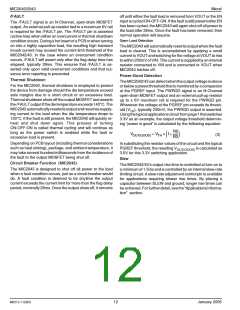
The graphs below (Figure 3) display the current limit factor
characteristic over the full temperature range at the indicated
voltage. These curves can be used as a point of reference in
determining the maximum variation in the device’s current
limit over the full temperature range. For example: With
Enable Input
Enable, the ON/OFF control for the output switch, is a digital
input available as an active-high (–1) or active-low (–2)
signal. TheENpin, referencedtoapproximately0.5× VBIAS,
must be driven to a clearly defined logic high or logic low.
Failure to observe this requirement, or allowing EN to float,
will cause the MIC2042/43 to exhibit unpredictable behavior.
EN should not be allowed to go negative with respect to
ground, nor allowed to exceed VBIAS. Failure to adhere to
these conditions may result in damage to the device.
V
(R
= V
= 3.0V and a nominal 2A current limit
IN
BIAS
= 192Ω), the low and high current limit settings for the
SET
MIC2042/43 would be 1.66A and 2.34A, respectively, as
shown on the 3V graph using the 192Ω reference point.
When current limiting occurs, the MIC2042 and MIC2043
respond differently. Upon first reaching the limiting current
both devices restrict current flow, allowing the load voltage to
drop below V . If the VIN-to-VOUT differential voltage ex-
IN
Undervoltage Lockout
ceeds 200mV, then a fault condition is declared and the fault
delaytimerisstarted.Ifthefaultconditionpersistslongerthan
the delay period, typically 28ms, then the /FAULT output
asserts low. At this point, the MIC2042 will continue to supply
When the switch is enabled, undervoltage lockout (UVLO)
monitors the input voltage, V , and prevents the output
IN
MOSFET from turning on until V exceeds a predetermined
IN
level, nominally set at 1.45V. The UVLO threshold is adjust-
ableandcanbevariedbyapplyinganexternalresistordivider
to the UVLOIN pin from VIN to GND. The resistive divider
networkisrequiredwhentheinputvoltageisbelow1.5V. The
UVLO threshold is internally preset to 1.45V if the UVLOIN
pin is left open. See “Applications Information” section.
current to the load at the limiting value (I
MIC2043 will latch off its output.
), whereas the
LIMIT
Current Limit
Current Limit
Current Limit
vs. R
vs. R
vs. R
SET
SET
SET
4
3.5
3
4
3.5
3
4
3.5
3
–40°C to +85°C
VIN = VBIAS = 5V
–40°C to +85°C
VIN = VBIAS = 3V
–40°C to +85°C
VIN = VBIAS = 1.6V
2.5
2
2.5
2
2.5
2
CLF (HI)
CLF (HI)
CLF (HI)
1.5
1
1.5
1
1.5
1
CLF (LO)
CLF (LO)
0.5
0
0.5
0
0.5
0
CLF (LO)
0
120 240 360 480 600 720 840 960
(Ω)
0
120 240 360 480 600 720 840 960
(Ω)
0
120 240 360 480 600 720 840 960
(Ω)
R
R
R
SET
SET
SET
Figure 3. Current Limit Factor
January 2005
11
M0512-112603

 MICREL [ MICREL SEMICONDUCTOR ]