Micrel, Inc.
KSZ9021RL/RN
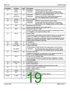
Pin Number
Pin Name
RXD0 /
Type(1)
Pin Function
RGMII Mode:
Config Mode:
32
I/O
RGMII RD0 (Receive Data 0) Output /
MODE0
The pull-up/pull-down value is latched as MODE0 during
power-up / reset. See “Strapping Options” section for details.
33
RX_DV /
I/O
RGMII Mode:
Config Mode:
RGMII RX_CTL (Receive Control) Output /
CLK125_EN
Latched as CLK125_NDO Output Enable during power-up /
reset. See “Strapping Options” section for details.
34
35
DVDDH
RX_CLK /
PHYAD2
P
3.3V / 2.5V digital VDD
I/O
RGMII Mode:
Config Mode:
RGMII RXC (Receive Reference Clock) Output /
The pull-up/pull-down value is latched as PHYAD[2] during
power-up / reset. See “Strapping Options” section for details.
36
37
MDC
Ipu
Management Data Clock Input
This pin is the input reference clock for MDIO (pin 37).
Management Data Input / Output
MDIO
Ipu/O
This pin is synchronous to MDC (pin 36) and requires an external pull-up resistor
to 3.3V digital VDD in a range from 1.0KΩ to 4.7KΩ.
38
INT_N
O
Interrupt Output
This pin provides a programmable interrupt output and requires an external pull-up
resistor to 3.3V digital VDD in a range from 1.0KΩ to 4.7KΩ when active low.
Register 1Bh is the Interrupt Control/Status Register for programming the interrupt
conditions and reading the interrupt status. Register 1Fh bit 14 sets the interrupt
output to active low (default) or active high.
39
40
41
DVDDL
DVDDH
P
P
1.2V digital VDD
3.3V / 2.5V digital VDD
CLK125_NDO /
I/O
125MHz Clock Output
This pin provides a 125MHz reference clock output option for use by the MAC. /
LED_MODE
RESET_N
Config Mode:
The pull-up/pull-down value is latched as LED_MODE during
power-up / reset. See “Strapping Options” section for details.
42
43
Ipu
O
Chip Reset (active low)
Hardware pin configurations are strapped-in at the de-assertion (rising edge) of
RESET_N. See “Strapping Options” section for more details.
LDO_O
On-chip 1.2V LDO Controller Output
This pin drives the input gate of a P-channel MOSFET to generate 1.2V for the
chip’s core voltages. If 1.2V is provided by the system and this pin is not used, it
can be left floating.
44
45
AVDDL_PLL
XO
P
1.2V analog VDD for PLL
O
25MHz Crystal feedback
This pin is a no connect if oscillator or external clock source is used.
Crystal / Oscillator / External Clock Input
25MHz +/-50ppm tolerance
46
XI
I
47
48
AVDDH
ISET
P
3.3V analog VDD
I/O
Set transmit output level
Connect a 4.99KΩ 1% resistor to ground on this pin.
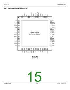
Exposed Paddle on bottom of chip
Connect P_GND to ground.
PADDLE
P_GND
Gnd
M9999-101309-1.1
October 2009
19

 MICREL [ MICREL SEMICONDUCTOR ]