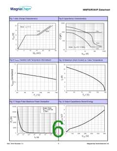
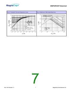
MMF60R360P Datasheet
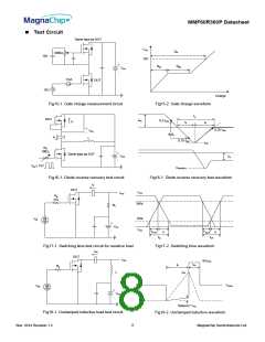
Test Circuit
Same type as DUT
VGS
Qg
100KΩ
10V
10V
+
-
Qgs
Qgd
VDS
1mA
DUT
10V
Charge
Fig15-2. Gate charge waveform
Fig15-1. Gate charge measurement circuit
trr
DUT
IFM
0.5 IRM
IF
ta
tb
+
-
0.25 IRM
VDS
di/dt
IS
L
0.75 IRM
IRM
Rg
10KΩ
+
-
Same type as DUT
VDD
VR
Vgs ± 15V
VRM(REC)
Fig16-1. Diode reverse recovery test circuit
Fig16-1. Diode reverse recovery test waveform
ID
DUT
VDS
VDS
Rg
25Ω
90%
RL
10%
VGS
Vgs
tp
+
VDD
-
Td(on)
tr
Td(off)
toff
tf
ton
Fig17-1. Switching time test circuit for resistive load
Fig17-2. Switching time waveform
IAS
DUT
VDS
BVDSS
tp
tAV
Rg
L
IAS
VDD
VDS(t)
Vgs
tp
+
VDD
-
Rds(on) * IAS
Fig18-1. Unclamped inductive load test circuit
Fig18-2. Unclamped inductive waveform
8
Nov. 2014 Revision 1.2
MagnaChip Semiconductor Ltd.

 MGCHIP [ MagnaChip ]