8 External Data Memory Accessing
As described in Section 5.2, to access the external data memory, the EXTRAM bit should be set to 1. Accesses
to external data memory can use either a 16-bit address (using ‘MOVX @DPTR’) or an 8-bit address (using
‘MOVX @Ri’), as described below.
Accessing by an 8-bit address
8-bit addresses are often used in conjunction with one or more other I/O lines to page the RAM. If an 8-bit
address is being used, the contents of the Port 2 SFR remain at the Port 2 pins throughout the external
memory cycle. This will facilitate paging access. Figure 5-5 shows an example of a hardware configuration for
accessing up to 2K bytes of external RAM. Port 0 serves as a multiplexed address/data bus to the RAM, and
3 lines of Port 2 are being used to page the RAM. The CPU generates /RD and /WR (alternate functions of
P3.7 and P3.6) to strobe the memory. Of course, the user may use any other I/O lines instead of P2 to page
the RAM.
Accessing by a 16-bit address
16-bit addresses are often used to access up to 64k bytes of external data memory. Figure 5-6 shows the
hardware configuration for accessing 64K bytes of external RAM. Whenever a 16-bit address is used, in
addition to the functioning of P0, /RD and /WR, the high byte of the address comes out on Port 2 and it is held
during the read or write cycle.
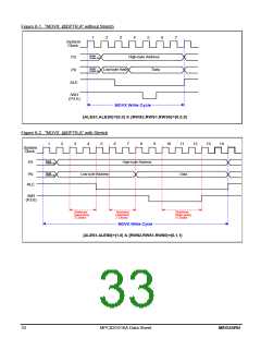
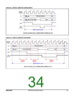
In any case, the low byte of the address is time-multiplexed with the data byte on Port 0. ALE (Address Latch
Enable) should be used to capture the address byte into an external latch. The address byte is valid at the
negative transition of ALE. Then, in a write cycle, the data byte to be written appears on Port 0 just before /WR is
activated, and remains there until after /WR is deactivated. In a read cycle, the incoming byte is accepted at Port
0 just before the read strobe is deactivated. During any access to external memory, the CPU writes 0FFH to the
Port 0 latch (the Special Function Register), thus obliterating whatever information the Port 0 SFR may have
been holding.
8.1 ALE-Pin Configuration
For the MPC82G516A, there is no dedicated pin for ALE signal. The ALE becomes an alternate function of P3.5
or P4.1, which can be selected by control bits P35ALE and P41ALE in the AUXR register, as shown below. And,
although an 80C51 MCU always outputs the ALE signal even there in no external accessing, the device doesn’t
output any ALE signal except when accessing the external data memory (EXTRAM=1).
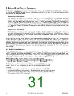
AUXR (Address=8EH, Auxiliary Register, Reset Value=0000, xx0xB)
7
6
5
4
3
2
1
0
-
URTS
ADRJ
P41ALE P35ALE
-
-
EXTRAM
P41ALE: when set, P4.1 functions as the ALE pin for external MOVX accessing.
P35ALE: when set, P3.5 functions as the ALE pin for external MOVX accessing.
EXTRAM:
0: Disable accessing to external data memory while address less than 0x0400;
Accessing of addresses 0x0000~0x03FF are automatically switched to on-chip XRAM.
1: Enable accessing to whole external data memory with addresses 0x0000~0xFFFF;
Accessing of on-chip XRAM is disabled.
31
MPC82G516A Data Sheet
MEGAWIN

 MEGAWIN [ MEGAWIN TECHNOLOGY CO., LTD ]