MX66C256
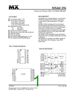
PIN DESCRIPTIONS
A0-A14 Address Input
These 15 address input select one of the 32768 x 8-bit words
in the RAM
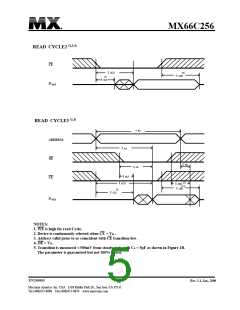
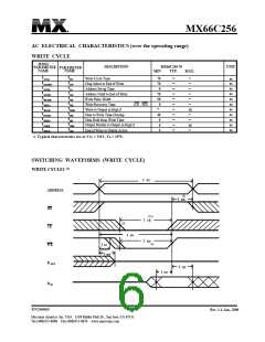
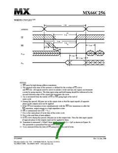
CE Chip Enable Input
CE is active LOW . Chip enable must be active to read from
or write to the device. If chip enable is not active, the device
is deselected and is in a standby power mode. The DQ pins will
be in the high impedance state when the device is deselected.
The write enable input is active LOW and controls read and
write operations. With the chip selected, when WE is HIGH
and OE is LOW, output data will be present on the DQ pins;
when WE is LOW, the data present on the DQ pins will be
written into the selected memory location.
WE Write Enable Input
OE Output Enable Input
The output enable input is active LOW. If the output enable
is active while the chip is selected and the write enable is
inactive, data will be present on the DQ pins and they will
be enabled. The DQ pins will be in the high impedance
state when OE is inactive.
DQ0 - DQ7 Data Input/Output Ports
These 8 bi-directional ports are used to read data from or
write data into the RAM.
Vcc
Power Supply
GND
Ground
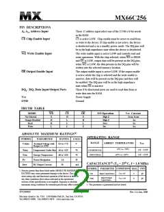
TRUTH TABLE
MODE
Not Selected
Output Disabled
Read
WE
X
CE
H
OE
X
I/O Operation
High Z
Vcc Current
ICCSB, ICCSB1
H
L
H
High Z
ICC
ICC
ICC
H
L
L
DOUT
Write
L
L
X
DIN
ABSOLUTE MAXIMUM RATINGS(1)
OPERATING RANGE
SYMBOL
PARAMETER
RATING
UNITS
V
RANGE
AMBIEN TEMPERATURE
Vcc
VTERM
Terminal Voltage with
Respect to GND
-0.5 to +7.0
0O C to + 70O
-40O C to + 85O
C
4.5 ~ 5.5V
4.5 ~ 5.5V
COMMERCIAL
INDUSTRIAL
TBIAS
TSTG
PT
Temperature Under Bias -40 to +125
OC
OC
W
C
Storage Temperature
Power Dissipation
DC Output Current
-60 to +150
1.0
20
CAPACITANCE(1) (TA = 25O C, f = 1.0 MHz)
IOUT
mA
SYMBOL
CONDITIONS MAX. UNIT
PARAMETER
1. Stresses greater than those listed under ABSOLUTE MAXIMUM
RATINGS may cause permanent damage to the device. This is a
stress rating only and functional operation of the device at these or
any other conditions above those indicated in the operational
sections of this specification is not implied. Exposure to absolute
CIN
Input Capacitance
V
IN = 0V
6
8
pF
pF
Input/Output
Capacitance
CDQ
V
I/O = 0V
1. This parameter is guaranteed and not tested.
maximum rating conditions for extended periods may affect reliability.
P/N DS0035
Rev. 1.1, Jan., 2000
2
Macronix America Inc. USA 1338 Ridder Park Dr., San Jose, CA 95131
Tel (408)453-8088 Fax (408)451-0876 www.macronix.com

 Macronix [ MACRONIX INTERNATIONAL ]