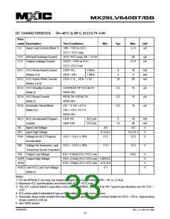
MX29LV640BT/BB
DC CHARACTERISTICS
TA=-40°C to 85° C, VCC=2.7V~3.6V
Para-
meter Description
Test Conditions
Min.
Typ.
Max.
Unit
I LI
Input Load Current (Note 1)
VIN = VSS to VCC ,
VCC = VCC max
±1.0
uA
I LIT A9 Input Leakage Current
I LO Output Leakage Current
VCC=VCC max; A9 = 12.5V
VOUT = VSS to VCC ,
VCC=VCC max
35
uA
uA
±1.0
ICC1 VCC Active Read Current
(Notes 2,3)
CE#= VIL,
OE# = VIH
5 MHz
1 MHz
9
2
16
4
mA
mA
mA
ICC2 VCC ActiveWrite Current
(Notes 2,4,6)
CE#= V IL , OE# = V IH
26
30
ICC3 VCC Standby Current
(Note 2)
CE#,RESET#=VCC±0.3V
WP#=VIH
0.2
0.2
0.2
15
15
15
uA
uA
uA
ICC4 VCC Reset Current
(Note 2)
RESET#=VSS±0.3V
WP#=VIH
ICC5 Automatic Sleep Mode
(Note 2,5)
VIL = V SS ± 0.3 V,
VIH = VCC ±0.3 V,
WP#=VIH
IACC ACC Accelerated Program
Current
CE#=VIL,
OE#=VIH
ACC pin
VCC pin
5
10
30
mA
mA
V
15
VIL
Input LowVoltage
-0.5
0.7xVcc
11.5
0.8
VIH Input HighVoltage
VHH Voltage for ACC Program
Acceleration
Vcc+0.3
12.5
V
VCC = 3.0 V ±10%
VCC = 3.0 V ±10%
V
VID Voltage for Autoselect and
Temporary Sector Unprotect
VOL Output LowVoltage
VOH1 Output HighVoltage
VOH2
11.5
12.5
0.45
V
IOL= 4.0mA,VCC=VCC min
V
V
V
V
IOH=-2.0mA,VCC=VCC min 0.85VCC
IOH=-100uA,VCC=VCC min VCC-0.4
1.5
VLKO LowVCC Lock-OutVoltage
(Note 4)
Notes:
1. On the WP#/ACC pin only, the maximum input load current when WP# = VIL is ±5.0uA.
2. Maximum ICC specifications are tested with VCC = VCC max.
3. The ICC current listed is typically is less than 2 mA/MHz, with OE# at VIH. Typical specifications are for VCC =
3.0V.
4. ICC active while Embedded Erase or Embedded Program is in progress.
5. Automatic sleep mode enables the low power mode when addresses remain stable for t ACC + 30 ns.Typical sleep
mode current is 200 nA.
6. Not 100% tested.
P/N:PM1076
REV. 1.2, SEP. 07, 2005
33

 Macronix [ MACRONIX INTERNATIONAL ]