MX25L12835F
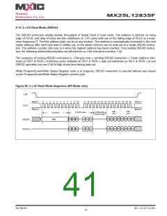
9-13. 2 x I/O Read Mode (2READ)
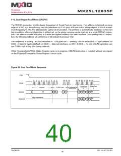
The 2READ instruction enable double throughput of Serial Flash in read mode. The address is latched on rising
edge of SCLK, and data of every two bits (interleave on 2 I/O pins) shift out on the falling edge of SCLK at a maxi-
mum frequency fT. The first address byte can be at any location. The address is automatically increased to the next
higher address after each byte data is shifted out, so the whole memory can be read out at a single 2READ instruc-
tion. The address counter rolls over to 0 when the highest address has been reached. Once writing 2READ instruc-
tion, the following address/dummy/data out will perform as 2-bit instead of previous 1-bit.
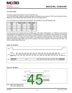
The sequence of issuing 2READ instruction is: CS# goes low sending 2READ instruction 3-byte address inter-
→
→
leave on SIO1 & SIO0 4 dummy cycles (default) on SIO1 & SIO0 data out interleave on SIO1 & SIO0 to end
→
→
→
2READ operation can use CS# to high at any time during data out.
While Program/Erase/Write Status Register cycle is in progress, 2READ instruction is rejected without any impact
on the Program/Erase/Write Status Register current cycle.
Figure 29. 2 x I/O Read Mode Sequence (SPI Mode only)
CS#
Mode 3
Mode 0
Mode 3
Mode 0
0
1
2
3
4
5
6
7
8
9
10
17 18 19 20 21 22 23 24 25 26 27 28 29 30
SCLK
Data
Data
Configurable
Dummy Cycle
12 ADD Cycles
Command
Out 1
Out 2
D6 D4 D2 D0 D6 D4 D2 D0
A22 A20 A18
A23 A21 A19
A4 A2 A0
BBh
SI/SIO0
D7 D5 D3 D1 D7 D5 D3 D1
A5 A3 A1
SO/SIO1
P/N: PM1795
REV. 1.0, OCT. 23, 2012
41

 Macronix [ MACRONIX INTERNATIONAL ]