MX29F080
SET-UP AUTOMATIC CHIP/SECTOR ERASE
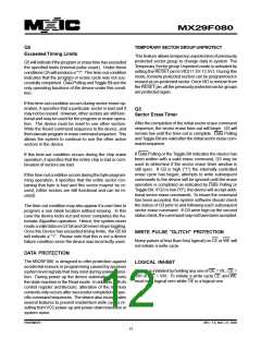
READ/RESET COMMAND
Chip erase is a six-bus cycle operation. There are two
"unlock" write cycles. These are followed by writing the
"set-up" command 80H. Two more "unlock" write cycles
are then followed by the chip erase command 10H.
The read or reset operation is initiated by writing the
read/reset command sequence into the command reg-
ister. Microprocessor read cycles retrieve array data.
The device remains enabled for reads until the command
register contents are altered.
The Automatic Chip Erase does not require the device
to be entirely pre-programmed prior to executing the Au-
tomatic Chip Erase. Upon executing the Automatic Chip
Erase, the device will automatically program and verify
the entire memory for an all-zero data pattern. When the
device is automatically verified to contain an all-zero
pattern, a self-timed chip erase and verify begin. The
erase and verify operations are completed when the data
on Q7 is "1" at which time the device returns to the Read
mode. The system is not required to provide any control
or timing during these operations.
If program-fail or erase-fail happen, the write of F0H will
reset the device to abort the operation. A valid com-
mand must then be written to place the device in the
desired state.
SILICON-ID-READ COMMAND
Flash memories are intended for use in applications where
the local CPU alters memory contents. As such, manu-
facturer and device codes must be accessible while the
device resides in the target system. PROM program-
mers typically access signature codes by raising A9 to
a high voltage. However, multiplexing high voltage onto
address lines is not generally desired system design
practice.
When using the Automatic Chip Erase algorithm, note
that the erase automatically terminates when adequate
erase margin has been achieved for the memory array
(no erase verification command is required).
If the Erase operation was unsuccessful, the data on Q5
is "1" (see Table 4), indicating the erase operation ex-
ceed internal timing limit.
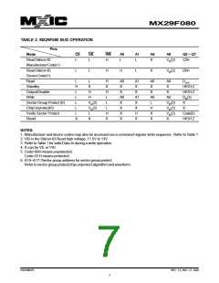
The MX29F080 contains a Silicon-ID-Read operation to
supplement traditional PROM programming methodol-
ogy. The operation is initiated by writing the read silicon
ID command sequence into the command register. Fol-
lowing the command write, a read cycle with
A1=VIL,A0=VIL retrieves the manufacturer code of C2H.
A read cycle with A1=VIL, A0=VIH returns the device
code of D5H for MX29F080.
The automatic erase begins on the rising edge of the
lastWE pulse in the command sequence and terminates
when the data on Q7 is "1" and the data on Q6 stops
toggling for two consecutive read cycles, at which time
the device returns to the Read mode.
TABLE 3. EXPANDED SILICON ID CODE
Pins
A0
A1
Q7
1
Q6
1
Q5
0
Q4
0
Q3
0
Q2
0
Q1
1
Q0
0
Code(Hex)
C2H
Manufacturecode
VIL VIL
Device code for MX29F080 VIH VIL
1
1
0
1
0
1
0
1
D5H
P/N:PM0579
REV. 1.6, NOV. 21, 2002
8

 Macronix [ MACRONIX INTERNATIONAL ]