MX29F080
AUTOMATIC PROGRAMMING
AUTOMATIC ERASE ALGORITHM
The MX29F080 is byte programmable using the Auto-
matic Programming algorithm. The Automatic Program-
ming algorithm makes the external system do not need
to have time out sequence nor to verify the data pro-
grammed. The typical chip programming time at room
temperature of the MX29F080 is less than 8 seconds.
MXIC's Automatic Erase algorithm requires the user to
write commands to the command register using stand-
ard microprocessor write timings. The device will auto-
matically pre-program and verify the entire array. Then
the device automatically times the erase pulse width,
provides the erase verification, and counts the number
of sequences. A status bit toggling between consecu-
tive read cycles provides feedback to the user as to the
status of the programming operation.
AUTOMATIC CHIP ERASE
The entire chip is bulk erased using 10 ms erase pulses
according to MXIC's Automatic Chip Erase algorithm.
Typical erasure at room temperature is accomplished in
less than 8 seconds. The Automatic Erase algorithm
automatically programs the entire array prior to electri-
cal erase. The timing and verification of electrical erase
are controlled internally within the device.
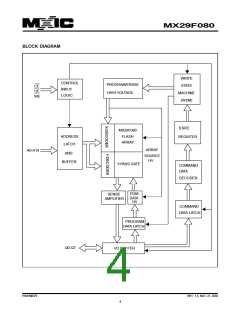
Register contents serve as inputs to an internal state-
machine which controls the erase and programming cir-
cuitry. During write cycles, the command register inter-
nally latches address and data needed for the program-
ming and erase operations. During a system write cycle,
addresses are latched on the falling edge, and data are
latched on the rising edge of WE or CE, whichever hap-
pens first .
MXIC's Flash technology combines years of EPROM
experience to produce the highest levels of quality, re-
liability, and cost effectiveness.The MX29F080 electri-
cally erases all bits simultaneously using Fowler-Nord-
heim tunneling. The bytes are programmed by using
the EPROM programming mechanism of hot electron
injection.
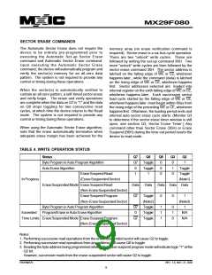
AUTOMATIC SECTOR ERASE
The MX29F080 is sector(s) erasable using MXIC's
Auto Sector Erase algorithm. Sector erase modes
allow sectors of the array to be erased in one erase
cycle. The Automatic Sector Erase algorithm
automatically programs the specified sector(s) prior to
electrical erase. The timing and verification of
electrical erase are controlled internally within the
device.
During a program cycle, the state-machine will control
the program sequences and command register will not
respond to any command set. During a Sector Erase
cycle, the command register will only respond to Erase
Suspend command. After Erase Suspend is completed,
the device stays in read mode. After the state machine
has completed its task, it will allow the command regis-
ter to respond to its full command set.
AUTOMATIC PROGRAMMING ALGORITHM
MXIC's Automatic Programming algorithm require the
user to only write program set-up commands (including
2 unlock write cycle and A0H) and a program command
(program data and address). The device automatically
times the programming pulse width, provides the pro-
gram verification, and counts the number of sequences.
A status bit similar to DATA polling and a status bit tog-
gling between consecutive read cycles, provide feed-
back to the user as to the status of the programming
operation.
P/N:PM0579
REV. 1.6, NOV. 21, 2002
5

 Macronix [ MACRONIX INTERNATIONAL ]