MX29F080
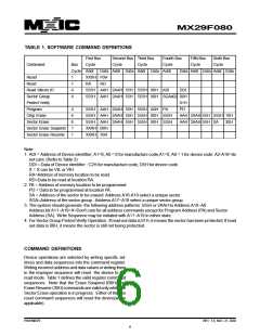
vice will automatically provide an adequate internally gen-
erated program pulse and verify margin.
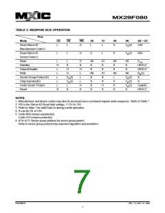
ERASE SUSPEND
This command only has meaning while the state ma-
chine is executing Automatic Sector Erase operation,
and therefore will only be responded during Automatic
Sector Erase operation. When the Erase Suspend com-
mand is written during a sector erase operation, the de-
vice requires a maximum of 100us to suspend the erase
operations.However,When the Erase Suspend command
is written during the sector erase time-out, the device
immediately terminates the time-out period and suspends
the erase operation. After this command has been ex-
ecuted, the command register will initiate erase suspend
mode. The state machine will return to read mode auto-
matically after suspend is ready. At this time, state ma-
chine only allows the command register to respond to
the Read Memory Array, Erase Resume and program
commands.
If the program operation was unsuccessful, the data on
Q5 is "1"(seeTable 4), indicating the program operation
exceed internal timing limit.The automatic programming
operation is completed when the data read on Q6 stops
toggling for two consecutive read cycles and the data
on Q7 and Q6 are equivalent to data written to these two
bits, at which time the device returns to the Read mode
(no program verify command is required).
DATA POLLING-Q7
The MX29F080 also features Data Polling as a method
to indicate to the host system that the Automatic Pro-
gram or Erase algorithms are either in progress or com-
pleted.
The system can determine the status of the program
operation using the Q7 or Q6 status bits, just as in the
standard program operation. After an erase-suspend pro-
gram operation is complete, the system can once again
read array data within non-suspended sector.
While the Automatic Programming algorithm is in opera-
tion, an attempt to read the device will produce the
complement data of the data last written to Q7. Upon
completion of the Automatic Program Algorithm an at-
tempt to read the device will produce the true data last
written to Q7. The Data Polling feature is valid after the
rising edge of the fourth WE or CE, whichever happens
first, of the four write pulse sequences for automatic
program.
ERASE RESUME
This command will cause the command register to clear
the suspend state and return back to Sector Erase mode
but only if an Erase Suspend command was previously
issued. Erase Resume will not have any effect in all
other conditions. Another Erase Suspend command can
be written after the chip has resumed erasing.
While the Automatic Erase algorithm is in operation, Q7
will read "0" until the erase operation is competed. Upon
completion of the erase operation, the data on Q7 will
read "1". The Data Polling feature is valid after the rising
edge of the sixth WE or CE, whichever happens first, of
six write pulse sequences for automatic chip/sector
erase.
SET-UP AUTOMATIC PROGRAM COMMANDS
To initiate Automatic Program mode, A three-cycle com-
mand sequence is required. There are two "unlock" write
cycles. These are followed by writing the Automatic Pro-
gram command A0H.
The Data Polling feature is active during Automatic Pro-
gram/Erase algorithm or sector erase time-out. (see sec-
tion Q3 Sector Erase Timer)
Once the Automatic Program command is initiated, the
nextWE pulse causes a transition to an active program-
ming operation. Addresses are latched on the falling
edge, and data are internally latched on the rising edge
of the WE or CE, whichever happens first pulse. The
rising edge of WE or CE, whichever happens first also
begins the programming operation. The system is not
required to provide further controls or timings. The de-
P/N:PM0579
REV. 1.6, NOV. 21, 2002
10

 Macronix [ MACRONIX INTERNATIONAL ]