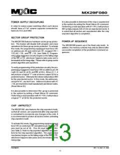
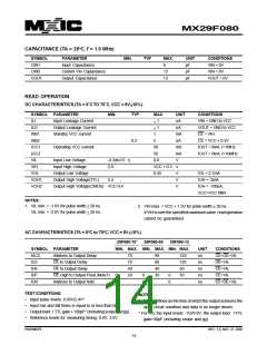
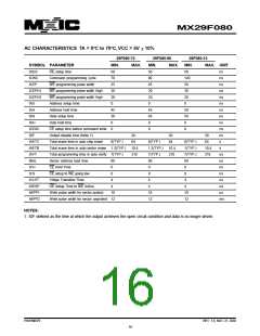
MX29F080
It is also possible to determine if the chip is unprotected
in the system by writing the Read Silicon ID command.
Performing a read operation with A1=VIH, it will produce
00H at data outputs (Q0-Q7) for an unprotected sector.It
is noted that all sectors are unprotected after the chip
unprotect algorithm is completed.
POWER SUPPLY DECOUPLING
In order to reduce power switching effect, each device
should have a 0.1uF ceramic capacitor connected be-
tween itsVCC and GND.
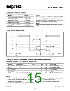
SECTOR GROUP PROTECTION
POWER-UP SEQUENCE
The MX29F080 features hardware sector group protec-
tion. This feature will disable both program and erase
operations for these group sector protected. To activate
this mode, the programming equipment must force VID
on address pin A9 and control pin OE, (suggest VID =
12V) A6 = VIL and CE = VIL. (see Table 2) Program-
ming of the protection circuitry begins on the falling edge
of the WE or CE, whichever happens later pulse and is
terminated on the rising edge. Please refer to group sector
protect algorithm and waveform.
The MX29F080 powers up in the Read only mode. In
addition, the memory contents may only be altered after
successful completion of the predefined command se-
quences.
To verify programming of the protection circuitry, the pro-
gramming equipment must forceVID on address pin A9
( with CE and OE atVIL and WE at VIH). When A1=1, it
will produce a logical "1" code at device output Q0 for a
protected sector. Otherwise the device will produce 00H
for the unprotected sector. In this mode, the addresses,
except for A1, are don't care. Address locations with A1
=VIL are reserved to read manufacturer and device codes.
(Read Silicon ID)
It is also possible to determine if the group is protected
in the system by writing a Read Silicon ID command.
Performing a read operation with A1=VIH, it will produce
a logical "1" at Q0 for the protected sector.
CHIP UNPROTECT
The MX29F080 also features the chip unprotect mode,
so that all sectors are unprotected after chip unprotect
is completed to incorporate any changes in the code. It
is recommended to protect all sectors before activating
chip unprotect mode.
To activate this mode, the programming equipment must
forceVID on control pin OE and address pin A9. The CE
pins must be set at VIL. Pins A6 must be set to VIH.
(seeTable 2) Refer to chip unprotect algorithm and wave-
form for the chip unprotect algorithm. The unprotection
mechanism begins on the falling edge of the WE or CE,
whichever happens later pulse and is terminated on the
rising edge.
P/N:PM0579
REV. 1.6, NOV. 21, 2002
13

 Macronix [ MACRONIX INTERNATIONAL ]