MX27L1000
SYSTEM CONSIDERATIONS
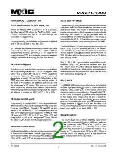
TWO-LINE OUTPUT CONTROL FUNCTION
During the switch between active and standby
conditions, transient current peaks are produced on the
rising and falling edges of Chip Enable. The magnitude
of these transient current peaks is dependent on the
outputcapacitanceloadingofthedevice. Ataminimum,
a0.1uFceramiccapacitor(highfrequency,lowinherent
inductance) should be used on each device between
Vcc and GND to minimize transient effects. In addition,
to overcome the voltage drop caused by the inductive
effects of the printed circuit board traces on EPROM
arrays, a 4.7 uF bulk electrolytic capacitor should be
usedbetweenVccandGNDforeacheightdevices. The
location of the capacitor should be close to where the
power supply is connected to the array.
To accommodate multiple memory connections, a two-
line control function is provided to allow for:
1. Low memory power dissipation,
2. Assurance that output bus contention will not
occur.
It is recommended that CE be decoded and used as
theprimarydevice-selectingfunction,whileOEbemade
a common connection to all devices in the array and
connected to the READ line from the system control
bus. This assures that all deselected memory devices
are in their low-power standby mode and that the output
pinsareonlyactivewhendataisdesiredfromaparticular
memory device.
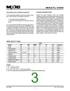
MODE SELECT TABLE
PINS
MODE
CE
OE
VIL
VIH
X
PGM
X
A0
X
A9
X
VPP
VCC
VCC
VCC
VCC
VPP
VPP
VPP
VCC
VCC
OUTPUTS
DOUT
High Z
High Z
High Z
DIN
Read
VIL
OutputDisable
Standby(TTL)
Standby(CMOS)
Program
VIL
X
X
X
VIH
X
X
X
VCC ±0.3V
VIL
X
X
X
X
VIH
VIL
X
VIL
VIH
X
X
X
ProgramVerify
ProgramInhibit
VIL
X
X
DOUT
High Z
C2H
VIH
X
X
ManufacturerCode(3) VIL
DeviceCode(3) VIL
VIL
VIL
X
VIL
VIH
VH
VH
X
0EH
NOTES:
1. VH = 12.0 V ±0.5 V
2. X = Either VIH or VIL
3. A1 - A8 = A10 - A16 = VIL(For auto select)
4. See DC Programming Characteristics for VPP voltage during programming.
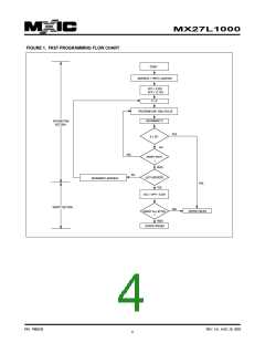
P/N: PM0238
REV. 3.8 , AUG. 26, 2003
3

 Macronix [ MACRONIX INTERNATIONAL ]