MX27L1000
FUNCTIONAL DESCRIPTION
AUTO IDENTIFY MODE
THE PROGRAMMING OF THE MX27L1000
Theautoidentifymodeallowsthereadingoutofabinary
code from an EPROM that will identify its manufacturer
and device type. This mode is intended for use by
programmingequipmentforthepurposeofautomatically
matching the device to be programmed with its
corresponding programming algorithm. This mode is
functional in the 25°C±5°C ambient temperature range
that is required when programming the MX27L1000.
When the MX27L1000 is delivered, or it is erased,
the chip has all 1M bits in the "ONE" or HIGH state.
"ZERO" are loaded into the MX27L1000 through the
procedure of programming.
For programming, the data to be programmed is applied
with 8 bits in parallel to the data pins.
Toactivatethismode,theprogrammingequipmentmust
force 12.0 ±0.5 V on address line A9 of the device.
Two identifier bytes may then be sequenced from the
device outputs by toggling address line A0 from VIL to
VIH. All other address lines must be held at VIL during
auto identify mode.
VCCmustbeappliedsimultaneouslyorbeforeVPP,and
removed simultaneously or after VPP.
When
programming an MXIC EPROM, a 0.1uF capacitor is
required across VPP and ground to suppress spurious
voltage transients which may damage the device.
Byte 0 ( A0 = VIL) represents the manufacturer code,
and byte 1 (A0 = VIH), the device identifier code. For
the MX27L1000, these two identifier bytes are given
intheModeSelectTable. Allidentifiersformanufacturer
and device codes will possess odd parity, with the MSB
(Q7) defined as the parity bit.
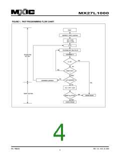
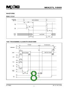
FASTPROGRAMMING
Thedeviceissetupinthefastprogrammingmodewhen
the programming voltage VPP = 12.75V is applied, with
VCC = 6.25 V and PGM = VIL(or OE = VIH) (Algorithm
is shown in Figure 1). The programming is achieved
by applying a single TTL low level 100us pulse to the
PGM input after addresses and data line are stable. If
the data is not verified, an additional pulse is applied
for a maximum of 25 pulses. This process is repeated
while sequencing through each address of the device.
When the programming mode is completed, the data in
all address is verified at VCC = VPP = 5V ±10%.
READ MODE
TheMX27L1000hastwo controlfunctions,bothofwhich
must be logically satisfied in order to obtain data at the
outputs. Chip Enable (CE) is the power control and
shouldbeusedfordeviceselection. OutputEnable(OE)
is the output control and should be used to gate data
to the output pins, independent of device selection.
Assuming that addresses are stable, address access
time(tACC)isequaltothedelayfromCEtooutput(tCE).
DataisavailableattheoutputstQEafterthefallingedge
of OE, assuming that CE has been LOW and addresses
have been stable for at least tACC - tOE.
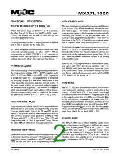
PROGRAM INHIBIT MODE
Programming of multiple MX27L1000s in parallel with
different data is also easily accomplished by using the
Program Inhibit Mode. Except for CE and OE, all like
inputs of the parallel MX27L1000 may be common. A
TTL low-level program pulse applied to an MX27L1000
CE input with VPP = 12.5 ±0.5 V and PGM LOW will
programthat MX27L1000. Ahigh-levelCEinputinhibits
the other MX27L1000s from being programmed.
STANDBY MODE
The MX27L1000 has a CMOS standby mode which
reducesthemaximumVCCcurrent to10uA. Itisplaced
in CMOS standby when CE is at VCC ±0.3 V. The
MX27L1000 also has a TTL-standby mode which
reduces the maximum VCC current to 0.25mA. It is
placed in TTL-standby when CE is at VIH. When in
standby mode, the outputs are in a high-impedance
state, independent of the OE input.
PROGRAM VERIFY MODE
Verificationshouldbeperformedontheprogrammedbits
to determine that they were correctly programmed. The
verification should be performed with OE and CE at VIL,
PGM at VIH, and VPP at its programming voltage.
P/N: PM0238
REV. 3.8 , AUG. 26, 2003
2

 Macronix [ MACRONIX INTERNATIONAL ]