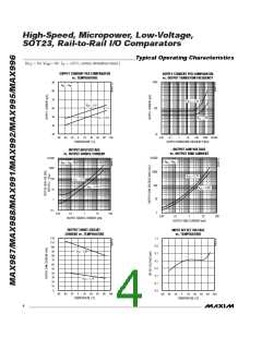
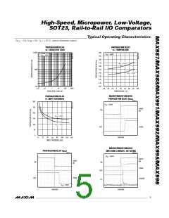
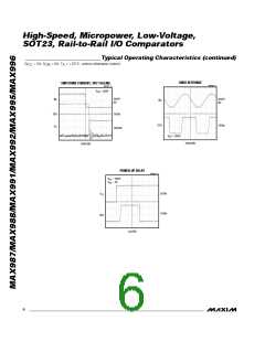
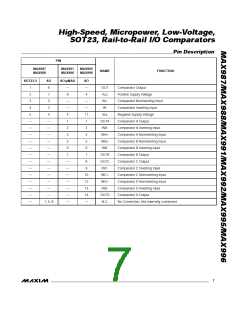
Hig h -S p e e d , Mic ro p o w e r, Lo w -Vo lt a g e ,
S OT2 3 , Ra il-t o -Ra il I/O Co m p a ra t o rs
78125/MAX96
5) Calculate R2 as shown. For this example, choose an
Us e the following p roc e d ure to c a lc ula te re s is tor
values:
8.2kΩ standard value:
1
1) Select R3 according to the formulas R3 = V
/ 1µA
REF
R2 =
or R3 = (V
- V ) / 1µA - R4. Use the smaller of
REF
CC
V
1
1
THR
x R1
−
−
the two resulting resistor values.
V
R1
R3
REF
2) Choose the hysteresis band required (V ). For this
HB
1
example, choose 50mV.
R2 =
= 8.03kΩ
3.0V
1.2 x 12kΩ
1
1
3) Calculate R1 according to the following equation:
−
−
12kΩ
2.2MΩ
R1 = (R3 + R4) x (V / V
)
HB
CC
6) Verify trip voltages and hysteresis as follows:
4) Choose the trip point for V rising (V
; V
is
IN
THR
THF
the trip point for V falling). This is the threshold
IN
voltage at which the comparator switches its output
1
1
1
from low to high as V rises above the trip point.
IN
V
rising : V
= V x R1 x
REF
+
+
IN
THR
R1
R2
R3
5) Calculate R2 as follows:
R1 x V
CC
1
V
falling : V
= V
−
IN
THF
THR
R2 =
R3
V
1
1
THR
x R1
−
−
Hysteresis = V
− V
THF
V
R1
R3 + R4
THR
REF
6) Verify trip voltages and hysteresis as follows:
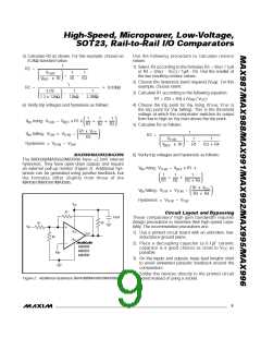
MAX988/MAX992/MAX996
The MAX988/MAX992/MAX996 have ±2.5mV internal
hysteresis. They have open-drain outputs and require
an external pull-up resistor (Figure 2). Additional hys-
teresis can be generated using positive feedback, but
the formula s d iffe r s lig htly from thos e of the
MAX987/MAX991/MAX995.
V
rising : V
= V x R1 x
REF
IN
THR
1
1
1
+
+
R1
R2
R3 + R4
R1 x V
CC
V
falling : V
= V
−
IN
THF
THR
R3 + R4
Hysteresis = V
− V
THF
THR
V
CC
R3
Circ u it La yo u t a n d Byp a s s in g
The s e c omp a ra tors ’ hig h-g a in b a nd wid th re q uire s
design precautions to maximize their high-speed capa-
bility. The recommended precautions are:
0.1µF
R4
R1
V
IN
V
CC
1) Use a printed circuit board with an unbroken, low-
inductance ground plane.
OUT
R2
V
EE
2) Place a decoupling capacitor (a 0.1µF ceramic
MAX988
MAX992
MAX996
capacitor is a good choice) as close to V
as
CC
V
REF
possible.
3) On the inputs and outputs, keep lead lengths short
to avoid unwanted parasitic feedback around the
comparators.
4) Solder the devices directly to the printed circuit
board instead of using a socket.
Figure 2. Additional Hysteresis (MAX988/MAX992/MAX996)
_______________________________________________________________________________________
9

 MAXIM [ MAXIM INTEGRATED PRODUCTS ]