Hig h -S p e e d , Mic ro p o w e r, Lo w -Vo lt a g e ,
S OT2 3 , Ra il-t o -Ra il I/O Co m p a ra t o rs
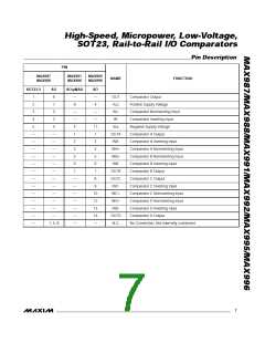
_______________De t a ile d De s c rip t io n
__________Ap p lic a t io n s In fo rm a t io n
The MAX987/MAX988/MAX991/MAX992/MAX995/
MAX996 are single/dual/quad low-power, low-voltage
comparators. They have an operating supply voltage
range between +2.5V and +5.5V and consume only
48µA per comparator, while achieving 120ns propaga-
tion delay. Their common-mode input voltage range
extends 0.25V beyond each rail. Internal hysteresis
ensures clean output switching, even with slow-moving
input signals. Large internal output drivers allow rail-to-
rail output swing with up to 8mA loads.
Ad d it io n a l Hys t e re s is
MAX987/MAX991/MAX995
The MAX987/MAX991/MAX995 have ±2.5mV internal
hysteresis. Additional hysteresis can be generated with
thre e re s is tors us ing p os itive fe e d b a c k (Fig ure 1).
Unfortuna te ly, this me thod a ls o s lows hys te re s is
response time. Use the following procedure to calcu-
late resistor values for the MAX987/MAX991/MAX995.
1) Select R3. Leakage current at IN is under 10nA;
therefore, the current through R3 should be at least
1µA to minimize errors caused by leakage current.
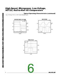
The output stage employs a unique design that mini-
mizes supply-current surges while switching, virtually
eliminating the supply glitches typical of many other
comparators. The MAX987/MAX991/MAX995 have a
push/pull output structure that sinks as well as sources
current. The MAX988/MAX992/MAX996 have an open-
The current through R3 at the trip point is (V
-
REF
V
) / R3. Considering the two possible output
OUT
states and solving for R3 yields two formulas: R3 =
/ 1µA or R3 = (V - V ) / 1µA. Use the
V
REF
REF
CC
s ma lle r of the two re s ulting re s is tor va lue s . For
example, if V = 1.2V and V = 5V, then the two
drain output stage that can be pulled beyond V to an
CC
REF
CC
absolute maximum of 6V above V
.
EE
R3 resistor values are 1.2MΩ and 3.8MΩ. Choose a
1.2MΩ standard value for R3.
In p u t S t a g e Circ u it ry
The devices’ input common-mode range extends from
2) Choose the hysteresis band required (V ). For this
HB
-0.25V to (V + 0.25V). These comparators may oper-
CC
example, choose 50mV.
ate at any differential input voltage within these limits.
Input bias current is typically 1.0pA if the input voltage
is between the supply rails. Comparator inputs are pro-
tected from overvoltage by internal body diodes con-
nected to the supply rails. As the input voltage exceeds
the supply rails, these body diodes become forward
biased and begin to conduct. Consequently, bias cur-
re nts inc re a s e e xp one ntia lly a s the inp ut volta g e
exceeds the supply rails.
3) Calculate R1 according to the following equation:
R1 = R3 x (V / V
)
HB
CC
For this example, insert the values R1 = 1.2MΩ x
(50mV / 5V) = 12kΩ.
4) Choose the trip point for V rising (V
; V
is
IN
THR
THF
the trip point for V falling). This is the threshold
IN
voltage at which the comparator switches its output
from low to high as V rises above the trip point. For
IN
Ou t p u t S t a g e Circ u it ry
The s e c omp a ra tors c onta in a uniq ue outp ut s ta g e
capable of rail-to-rail operation with up to 8mA loads.
Many comparators consume orders of magnitude more
current during switching than during steady-state oper-
ation. However, with this family of comparators, the
supply-current change during an output transition is
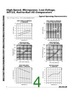
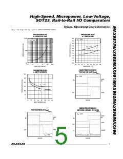
extremely small. The Typical Operating Characteristics
graph Supply Current vs. Output Transition Frequency
shows the minimal supply-current increase as the out-
put switching frequency approaches 1MHz. This char-
acteristic eliminates the need for power-supply filter
capacitors to reduce glitches created by comparator
switching currents. Battery life increases substantially
in high-speed, battery-powered applications.
this example, choose 3V.
V
CC
R3
R1
0.1µF
V
IN
V
CC
OUT
R2
V
EE
MAX987
MAX991
MAX995
V
REF
78125/MAX96
Figure 1. Additional Hysteresis (MAX987/MAX991/MAX995)
8
_______________________________________________________________________________________

 MAXIM [ MAXIM INTEGRATED PRODUCTS ]