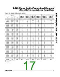
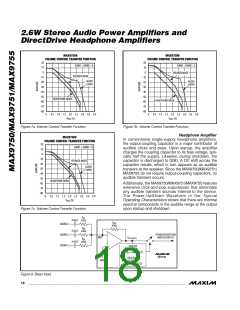
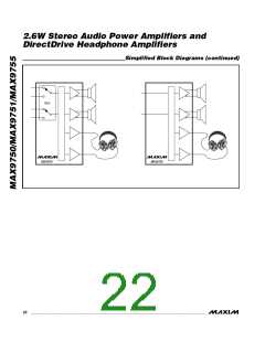
2.6W Stereo Audio Power Amplifiers and
DirectDrive Headphone Amplifiers
MAX9751/MAX9755 to provide the negative supply for
the headphone amplifiers. It can also be used to power
22µF
other devices within a design. Current draw from
OUTL+
CPV should be limited to 5mA, exceeding this affects
SS
1µF
1µF
OUTL-
the operation of the headphone amplifier. A typical
application is a negative supply to adjust the contrast
of LCD modules.
INL
INR
MAX9750
22µF
When considering the use of CPV
in this manner,
SS
OUTR+
OUTR-
note that the charge-pump voltage of CPV is roughly
SS
proportional to CPV
and is not a regulated voltage.
DD
The charge-pump output impedance plot appears in
the Typical Operating Characteristics.
20kΩ
20kΩ
10kΩ
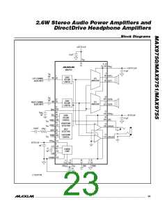
Layout and Grounding
Proper layout and grounding are essential for optimum
performance. Use large traces for the power-supply
inputs and amplifier outputs to minimize losses due to
parasitic trace resistance, as well as route head away
from the device. Good grounding improves audio per-
formance, minimizes crosstalk between channels, and
prevents any switching noise from coupling into the
audio signal. Connect CPGND, PGND and GND
together at a single point on the PC board. Route
CPGND and all traces that carry switching transients
away from GND, PGND, and the traces and compo-
nents in the audio signal path.
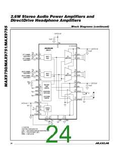
22nF
10kΩ
IN
10nF
MAX9711
OUT-
OUT+
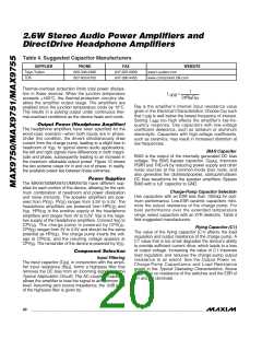
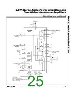
Figure 11. Stereo Plus Subwoofer Application Circuit
Connect all components associated with the charge
Output Capacitor (C2)
pump (C2 and C3) to the CPGND plane. Connect V
SS
The output capacitor value and ESR directly affect the
and CPV
together at the device. Place the charge-
SS
ripple at CPV . Increasing the value of C2 reduces
SS
pump capacitors (C1, C2, and C3) as close to the
device as possible. Bypass HPV and PV with a
output ripple. Likewise, decreasing the ESR of C2
reduces both ripple and output resistance. Lower
capacitance values can be used in systems with low
maximum output power levels. See the Output Power
vs. Charge-Pump Capacitance and Load Resistance
graph in the Typical Operating Characteristics.
DD
DD
0.1µF capacitor to GND. Place the bypass capacitors
as close to the device as possible.
Use large, low-resistance output traces. As load imped-
ance decreases, the current drawn from the device out-
puts increase. At higher current, the resistance of the
output traces decrease the power delivered to the load.
For example, when compared to a 0Ω trace, a 100mΩ
trace reduces the power delivered to a 4Ω load from
2.1W to 2W. Large output, supply, and GND traces also
improve the power dissipation of the device.
CPV
Bypass Capacitor
DD
The CPV
bypass capacitor (C3) lowers the output
DD
impedance of the power supply and reduces the
impact of the MAX9750/MAX9751/MAX9755’s charge-
pump switching transients. Bypass CPV
with C3, the
DD
same value as C1, and place it physically close to
CPV and PGND (refer to the MAX9750 Evaluation Kit
The MAX9750/MAX9751/MAX9755 thin QFN and
TSSOP-EP packages feature exposed thermal pads on
their undersides. This pad lowers the package’s ther-
mal resistance by providing a direct heat conduction
path from the die to the printed circuit board. Connect
the exposed thermal pad to GND by using a large pad
and multiple vias to the GND plane.
DD
for a suggested layout).
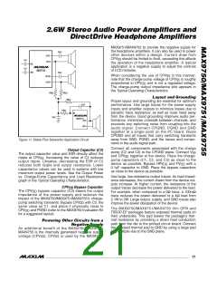
Powering Other Circuits from a
Negative Supply
An additional benefit of the MAX9750/MAX9751/
MAX9755 is the internally generated negative supply
voltage (CPV ). CPV
is used by the MAX9750/
SS
SS
______________________________________________________________________________________ 21

 MAXIM [ MAXIM INTEGRATED PRODUCTS ]